Seven-segment display (SSD)
Goal:
Be able to control a single and multiple SSD using microcontrollers.
Understand the operation of shift registers (74HC595N)
1.
SSD powered by SEVEN wires
A Seven-segment
display (SSD) unit is a simple LED package, typically all of
the
cathodes (negative terminals) or all of the anodes (positive terminals)
of the segment LEDs are connected and brought out to a common pin; this
is referred to as a "common cathode" or "common anode" device. The SSD
we are going to use in this lab is a 'common cathode' unit.

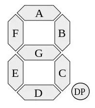
Fig. 1 The
internal connection (schematic) of the SSD in this lab
The decimal
number (1-10) in Fig. 1 are the pin numbers of the SSD unit. The
letters (A-G, DP) are the corresponding LEDs.
You can map the
schematic to the real SSD unit using Fig. 2, or directly check the
datasheet of the SSD (LSHD5503).
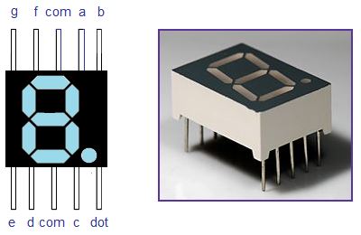
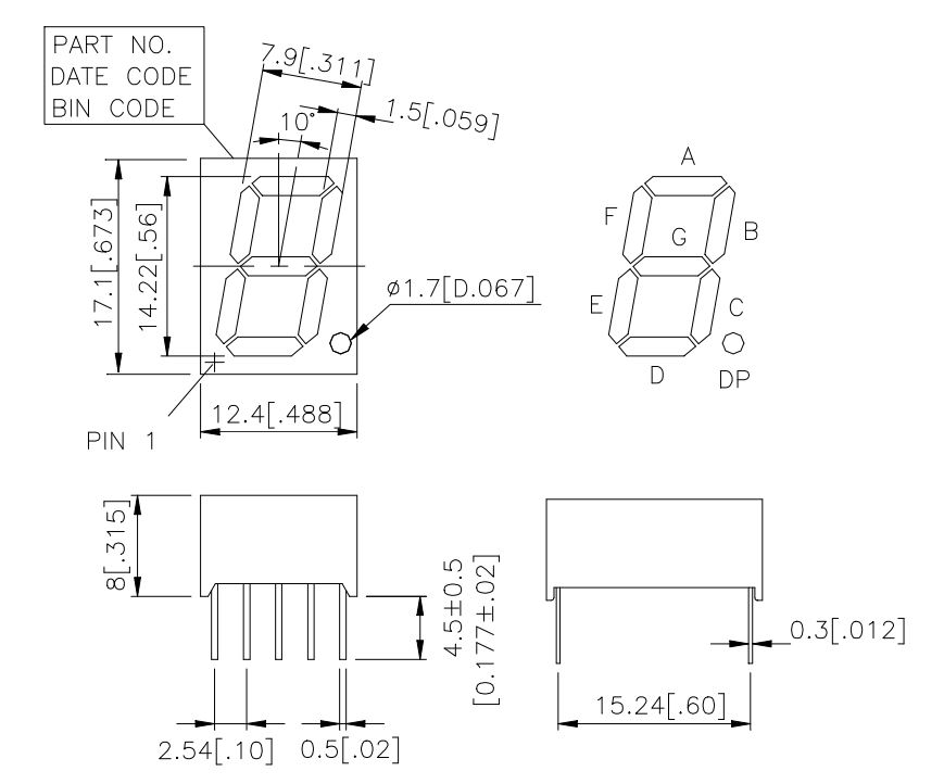
Fig. 2 SSD
pin/LED map.
With the LED/pin
map, you can power up the corresponding LEDs and display different
numbers and letters.
2.
Experiments
2.1 SSDs powered by individual
wires
Use the 5V
voltage supply on the Arduino Board
(do not go beyond that) as the power supply, connect the SSD pins to
resistors to limit the current (protect the SSD unit).

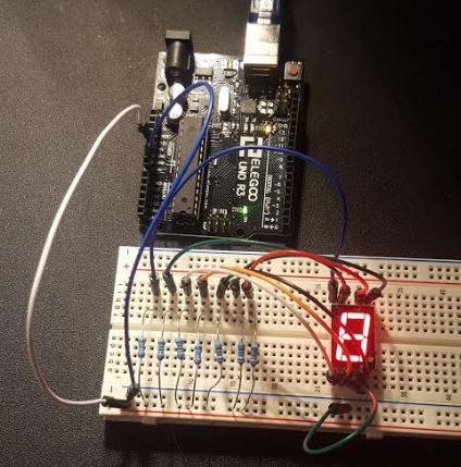
By
powering up a certain group of LEDs, try to display numbers
from 0, 1, 2, 3, ..., 9. The following figure shows you all
the LEDs in the SSD were powered up:
The
seven LEDs in the SSD device were individually controlled by SEVEN
wires. I can turn off a certian combination of wires to display a
number on it. Refer to the map again:
To display a '6'
there, I need to turn off 'B":
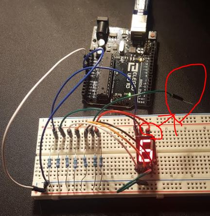
See the figure
above, I just plugged off one wire that used to be connected to 'B'.
Try to display
all the numbers from 0 - 9.
2.2
SSD powered by THREE wires (manually)
The
method in section 1 is definitely not good. It takes too much 'pin
resource' just to power up one single SSD device.
In this section, we'll use a Digital Decoder to control the SSD device.
We know that 3 bits can have 2^3=8 combinations. So we can simplify
the SSD control by using a 'decoder' which can convert your 3-bit input
code to an 8-bit code and drive the SSD indirectly.
We are going to
use M74HC4543 to drive our LED.
Connect 74HC4543
(the decoder) to your SSD:
('L' represents
GND, 'H' represents 5V)

Control
the SSD by change the voltage at A-D of the decoder, try to display 0,
1, 2, 3, ..., 9
Now,
you can create the same results but just control 4 pins instead of 7
pins. This is important because you saved a lot of pin resources, which
means you can save lots of space on a real circuit board!
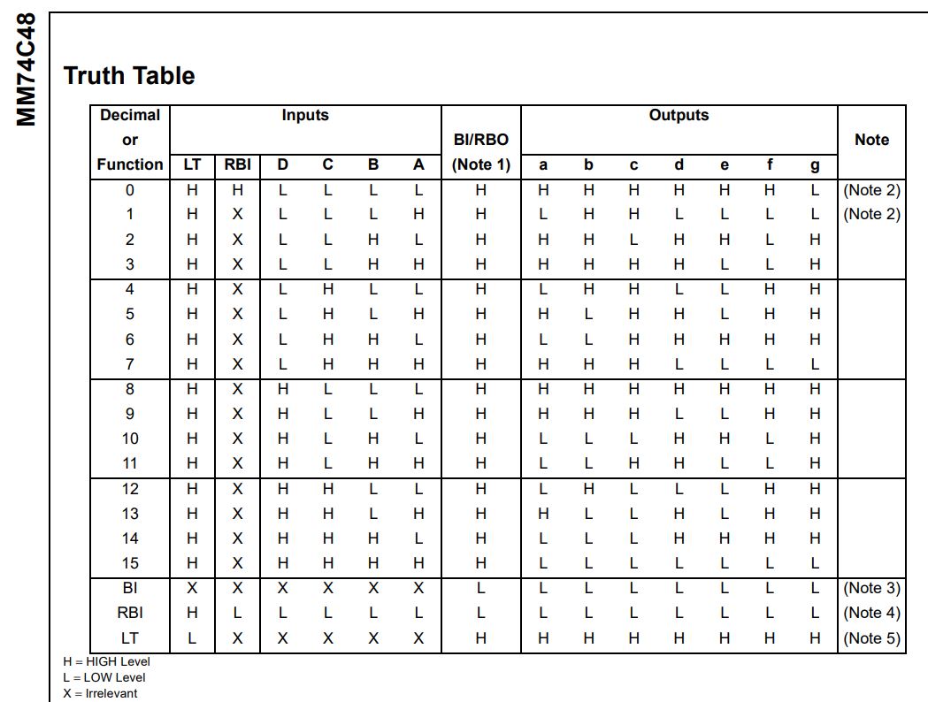
If you are using 74HC48, the connections would be slightly different. Please refer to the following snapshot from the datasheet to make the connections.
2.3
SSD
powerd by ONE wire (only one digital line to control all seven
pins)
In
this section, we'll use a 'shift register' integrated circuit (IC) to
receive the SSD control input SERIALLY, and then deliver all the code
to the SSD device in PARALLEL.
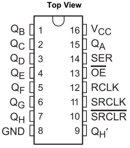
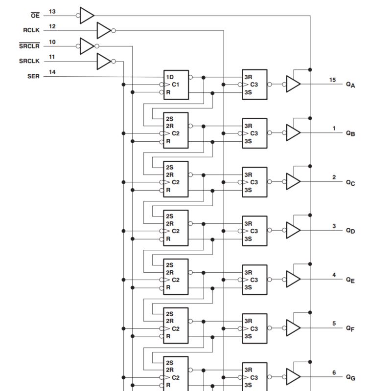
The top view of the 'shift register' can be found below:
74HC595N
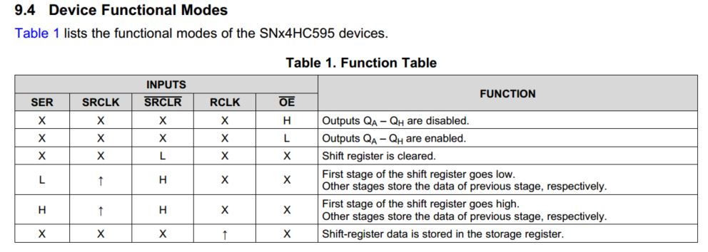
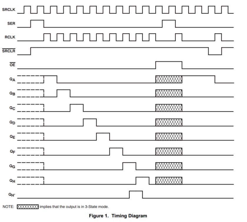
From
the internal circuit diagram below, we can tell that 'SER' is the one
SERIALLY deliver binary data to the first stage of Register, which will
be passed to the following ones. 'RCLK' seems like the 'Switch' for the
Parallel output. 'SRCLK' is used to shift the data being fed into the
first Register to the following ones.
The operation of
the shift register may seem difficult for you if you
don't have much 'digital logic' background.
Arduino has a
library/function called 'shiftOut()' can manage this job
for you if you don't want to handle the details of the sequential
logic.
Let's test the
shift register using simple LEDs first.
Make the
following connection to the hardware as shown below.

Use
the following code: (this is the example of using LSBFIRST):
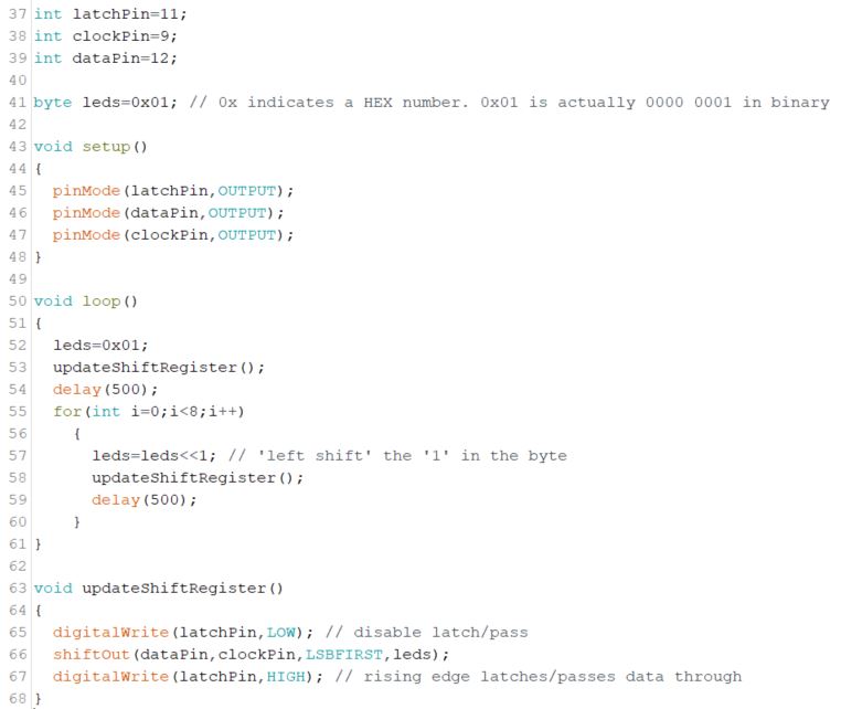
The
demonstration:
Make sure you
understand that the shifted LEDs you saw in the video are not shifted
by the 'shift refister' IC as what you saw. It is just changing it's
state every half seconds. The shift register shifted the data in
variable 'leds' to and latch them at the same time (in paralllel) to
the out put of the shift regfister: Q0 - Q7.
It might be
confusing that you are shifting the '1' in byte variable 'leds'. This
is done by an internal shift function inside the Arduino CPU. So there
are three things being 'shifted' but only the command
'shiftOut(dataPin,clockPin,LSBFIRST,leds)' is shifted by the 'shift
refister' IC we used here.
Now, we know how
to use the 74HC595N chip. There is only one
data line 'SER' instead of three or more. This is the strategy being
used in real-life. We can use this single 'shift register' IC to
control more than ONE SSD device, and even make a digital clock out of
it.
Let's display
decimal numbers to an SSD device using 74HC595N first (refer to the
schematic in the example above to wire up your cricuit) and use the
following code (please note the changes made in this code):
// SSD, single, counts, MSBFIRST, revised 9/16/2020
int latchPin=11;// RCLK
int clockPin=9;// SRCLK
int dataPin=12;//SER
byte SSDs=0x3F; // in binary, it is 0011 1111, which only turns off G
and H, will display 0
void setup()
{
pinMode(latchPin,OUTPUT);
pinMode(dataPin,OUTPUT);
pinMode(clockPin,OUTPUT);
}
void loop()
{
SSDs=0x06; //1
updateShiftRegister();
delay(500);
SSDs=0x5B; //2
updateShiftRegister();
delay(500);
SSDs=0x4F; //3
updateShiftRegister();
delay(500);
SSDs=0x66; //4
updateShiftRegister();
delay(500);
SSDs=0x6D; //5
updateShiftRegister();
delay(500);
SSDs=0x7D; //6
updateShiftRegister();
delay(500);
SSDs=0x07; //7
updateShiftRegister();
delay(500);
SSDs=0x7F; //8
updateShiftRegister();
delay(500);
SSDs=0x6F; //9
updateShiftRegister();
delay(500);
SSDs=0x3F; //0
updateShiftRegister();
delay(500);
}
void updateShiftRegister()
{
digitalWrite(latchPin,LOW); // disable latch/pass
shiftOut(dataPin,clockPin,MSBFIRST,SSDs);
digitalWrite(latchPin,HIGH); // rising edge latches/passes
data through
}
The 'delay(500)'
will
generate half second delay to detect if there is
any change in the SSD code. However, we don't have any changes in this
code, it is static, so the number on the SSD will not be changed.
If you want to
change it over
time, we should modify the code. For
example, let's make this counts from 0 to 9 and then back to 0.
Demonstration:
Of course you
can make the
delay shorter to roll it faster.
Repeat this
example first and then change it to LSBFIRST and modify the code
accordingly and demonstrate it in a video.
2.4
SSD
powerd by ONE wire (More than ONE SSD devices)
All the cathodes
are
connected together.

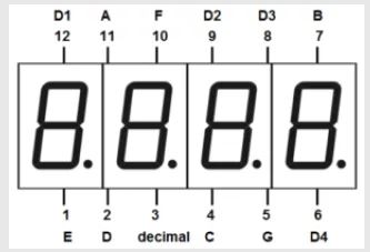
All
the 4 decimal digits are sharing the same A-G and DP. Every single
decimal digit can be enabled/disabled by turning on/off D1-D4.
If
we enable/disable everyone very quickly, your eye can't resolve the
change and it looks static. So we can display 4 different decimal
numbers at the 4 digits.
Let's try to
display '2019'
to the 4 digits.
Connect DIG1 -
DIG4 to pin7 -
pin4 on your Arduino board through 4 resistors.

(The
Arduino code is not provided)
Tasks:
1. Repeat/complete the work in Sections 2.1 - 2.4.