Homework 3 - Combinational Logic Blocks
Name: Taylor Schermer
Email: tschermer@fortlewis.edu
Task 1:
1. Repeat the simulation of Half
Adder and Full Adder in Section 1. Show the code, code explanations, and
simulation results in your report. (10 points)

Figure 1. Half Adder Code

Figure 2. Half Adder Simulation
The halfAdder module takes two inputs a and b, and produces two outputs s (sum) and c0 (carry). Inside the halfAdder module, the sum s is computed using the XOR operation (^) between a and b, while the carry c0 is computed using the AND operation (&) between a and b. The halfAdder_TB testbench initializes the inputs a and b with various combinations of values (0 and 1) and verifies the logic.

Figure 3. Full Adder Code

Figure 4. Full Adder Simulation
The FullAdder module takes three inputs a, b, and ci (carry in), and produces two outputs s (sum) and c0 (carry out). Inside the FullAdder module, the carry out c0 is computed using a combination of AND and XOR operations, while the sum s is computed using XOR operations. The FullAdder_TB testbench initializes the inputs a, b, and ci with different values (0 and 1) and iterates through all possible input combinations to test the logic via simulation.
Task 2:
2. Design the testbench for the
comparator in Section 2. Show the code, code explanations, and
simulation results in your report. (10 points)
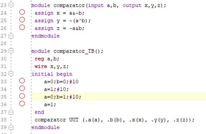
Figure 5. Comparator Code

Figure 6. Comparator Simulation
The comparator module takes two inputs a and b and produces three outputs x, y, and z, representing the results of different comparison operations. Inside the comparator module, each output is computed based on the logical operations between a and b. The comparator_TB testbench initializes the inputs a and b with various values (0 and 1) and verifies the functionality of the comparator module by observing the outputs x, y, and z.
Task 3:
3. Design the testbench for the 4-bit comparator in Section 3. Show the code, code explanations, and simulation results in your report. (10 points)
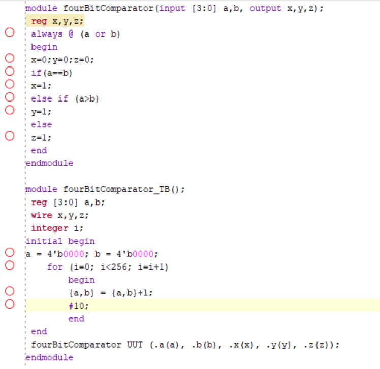
Figure 7. 4-Bit Comparator Code

Figure 8. 4-Bit Comparator Simulation Part 1

Figure 9. 4-Bit Comparator Simulation Part 2
The fourBitComparator module compares two four-bit inputs a and b and generates three outputs x, y, and z, indicating if a is equal to b, greater than b, or less than b, respectively. Inside the fourBitComparator module, the outputs are computed using conditional statements based on the comparison of a and b. The fourBitComparator_TB testbench initializes the inputs a and b with values from 0 to 15 and observes the outputs to verify the functionality of the fourBitComparator module.
Task 4:
4. Implement a 2-bit comparator on
the Basys 3 board. Use sw as inputs and led as outputs. Show the code,
code explanations, and an embedded Youtube video demonstration in your
report. (10 points)

Figure 10. 2-Bit Comparator Code
The twoBitComparator module takes two two-bit inputs a and b and generates three outputs x, y, and z, indicating if a is greater than (x), equal to (y), or less than (z) b. Inside the twoBitComparator module, the outputs are computed using bitwise operations based on the comparison of individual bits of a and b.
Task 5:
5. In Section 4, design the
testbench for the decoder and verify the logic in simulation (use the
Dataflow modeling method). Show the code, code explanations, and
simulation results in your report. (10 points)

Figure 11. Decoder Code

Figure 12. Decoder Simulation
The decoder module takes a two-bit input x and generates a four-bit output y, where each output represents a specific combination of input bits. Inside the decoder module, the outputs are computed using logical operations based on the states of individual input bits. The decoder_TB testbench initializes the input x with different binary values and observes the corresponding output y to verify the functionality of the decoder module.
Task 6:
6. In Section 5, for the 8x3
priority encoder, find Q2 and Q1, build the module and verify the logic
using simulations. Show the code, code explanations, and simulation
results in your report. (10 points)

Figure 13. 8x3 Priority Encoder Code Part 1

Figure 14. 8x3 Priority Encoder Code Part 2

Figure 15. 8x3 Priority Encoder Simulation
The eightToThreeEncoder module takes an eight-bit input d and generates a three-bit output q, encoding the active bit position of the input. The q output represents the position of the first active bit found in the input d, starting from the most significant bit. Inside the eightToThreeEncoder module, the output q is determined using a casex statement, which matches the input d against specific patterns and assigns the corresponding output value. The eightToThreeEncoder_tb testbench initializes the input d with different eight-bit values and observes the resulting output q to verify the functionality of the eightToThreeEncoder module
Task 7:
7. Derive the logic expression of
a 4-1 multiplexer. Show the process on a paper, insert it as an image
into your report. (10 points)

Figure 16. 4-1 Multiplexer Logic
Task 8:
8. In Section 6, implement a 4-1
multiplexer on your Basys 3 board. Show the code, code explanations, and
an embedded Youtube video demonstration in your report. (10 points)
This module (fourMUX) for implements a 4-to-1 multiplexer with four input signals (a, b, c, d), two select lines (s0, s1), and one output y. The output y is determined based on the select lines: if s1 is high, the output is either c or d, depending on the state of s0; otherwise, the output is either a or b, again depending on the state of s0. The testbench (fourMUX_TB) is for simulating the functionality of the 4-to-1 MUX module.

Figure 17. 4:1 MUX Code

Figure 18. 4:1 MUX Sim
There's a top-level module (fourMUX_TM) that connects switches to the inputs and select lines of the MUX and connects the output LED to display the selected signal.

Figure 19. 4:1 MUX Test Module Code
Task 9:
9. Design/verify an even parity
generator and checker in simulation respectively. Implement an even
parity checker on your Basys 3 board - use sw as inputs, use leds as
output indicators. Show the code, code explanations, and an embedded
Youtube video demonstration in your report. (10 points)

Figure 20. Parity Generator Code

Figure 21. Parity Generator Simulation
The parity generator module (parityGenerator) calculates the parity bit (y) of three input bits a, b, and c. The parity bit is computed as the XOR of the input bits. The testbench (parityGenerator_TB) verifies the logic. The test module (parityGenerator_TM) instantiates the parityGenerator module and connects it to switches (sw) as inputs and an LED (led) as the output, indicating the computed parity bit. This allows for testing the parity generation functionality on our Basys3 hardware by observing the LED output.

Figure 22. Parity Checker Code

Figure 23. Parity Checker Simulation
The parity checker module (parityChecker) verifies the parity of four input bits a, b, c, and d. The parity is determined by XORing the pairs of input bits (a with b, and c with d), and then XORing the results of these XOR operations. The output y indicates whether the parity is even (0) or odd (1). The testbench (parityChecker_TB) provides a simulation environment to test the parity checker functionality, while the test module (parityChecker_TM) instantiates the parityChecker module and connects it to switches (sw) as inputs and an LED (led) as the output for our Basys3.
Task 10:
10. Implement the design in
Section 8 and Section 9 on your Basys 3 board. Show embedded Youtube
video demonstration on your report. Show the code, code explanations,
and an embedded Youtube video demonstration in your report. (10
points)nd an embedded Youtube video demonstration in your report. (10
points)

Figure 24. Home Alarm System Updated Code
The homeAlarmDecoderSevenSegment module is a decoder that takes a 4-bit input and produces a 7-bit output, which corresponds to the pattern to display a number on a seven-segment display. Each input value maps to a specific pattern to represent a digit from 0 to 9, as well as a few letters (a, b, c, d, e, f). The homeAlarmSystem module is a part of a home alarm system. It takes a 4-bit input s representing the state of the alarm sensors, and a single-bit input m representing the mode of the alarm system. It produces a single-bit output a, indicating whether the alarm should be activated based on the sensor states and the mode. The homeAlarmSystem_TM module is a test module for the home alarm system. It connects the input switches (sw) to the sensor inputs and mode input, and the LED output to the output of the home alarm system. Additionally, it connects the seven-segment display (seg) and anode control (an) to the home alarm decoder to display the sensor states on the display.

Figure 25. Parking Count System Updated Code 1

Figure 26. Parking Count System Updated Code 2
The parkingCountSSD module is a decoder that takes a 4-bit input and produces a 7-bit output, which corresponds to the pattern to display a number on a seven-segment display. The parkingCount module calculates the count of parking spaces occupied based on a 9-bit input s, where each bit represents the occupancy status of a parking space (0 for empty, 1 for occupied). The count c is the sum of all the bits in the input. The parkingCount_tb module serves as a testbench for the parkingCount module. It connects the input switches (sw) to represent the occupancy status of parking spaces and the LED output (led) to display the count of occupied parking spaces in binary. Additionally, it connects the seven-segment display (seg) and anode control (an) to display the count on the display.