1. Verification of PCB
2. The purpose of this lab was to solder the PCB created in HW1
with all nessasary components to create a functional power distrobution
board. Similarly, the lab helped to reinforce the hands on nature of
PCB design.
3. Materials and Methods
GVIM computer
Application
Paper and Pencil
Vivado Application
4. Results
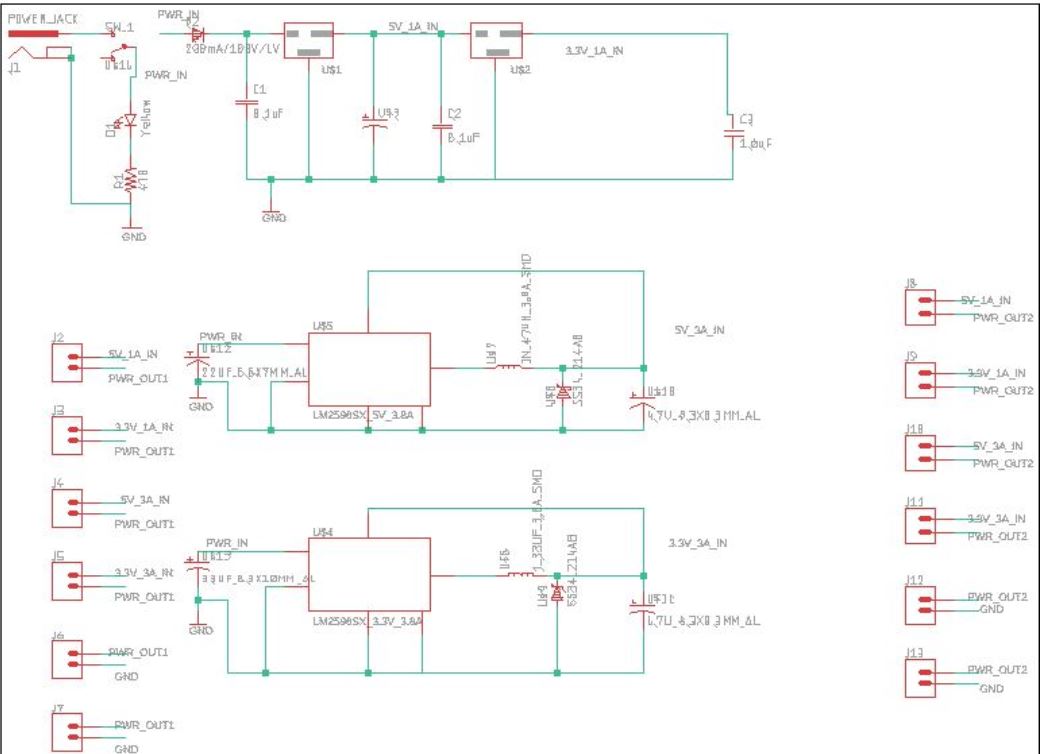
Figure 1. Schematic of the power distrobution board.
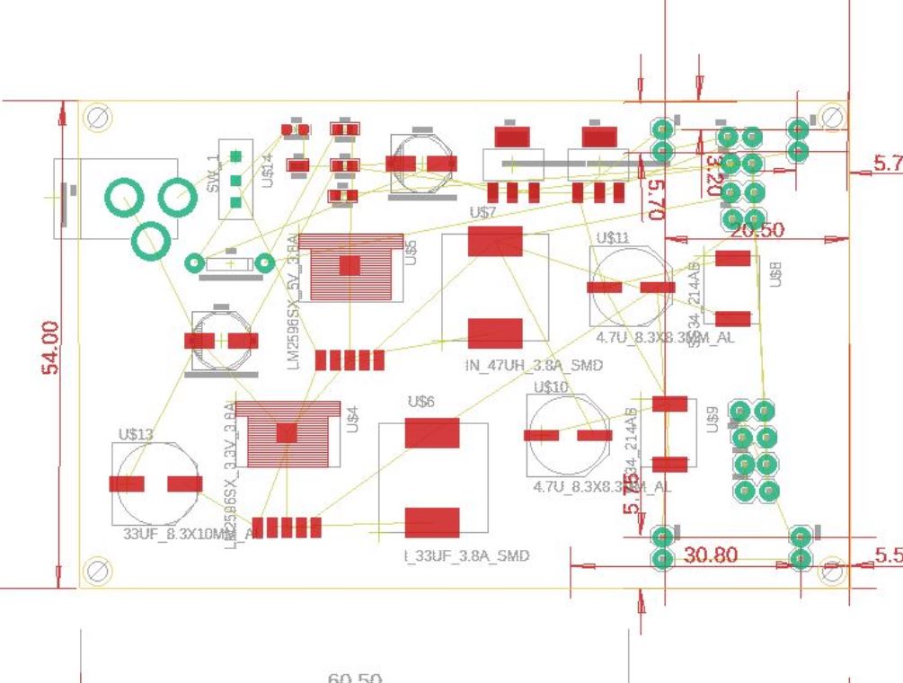
Figure 2. Layout of the power distrobution board.
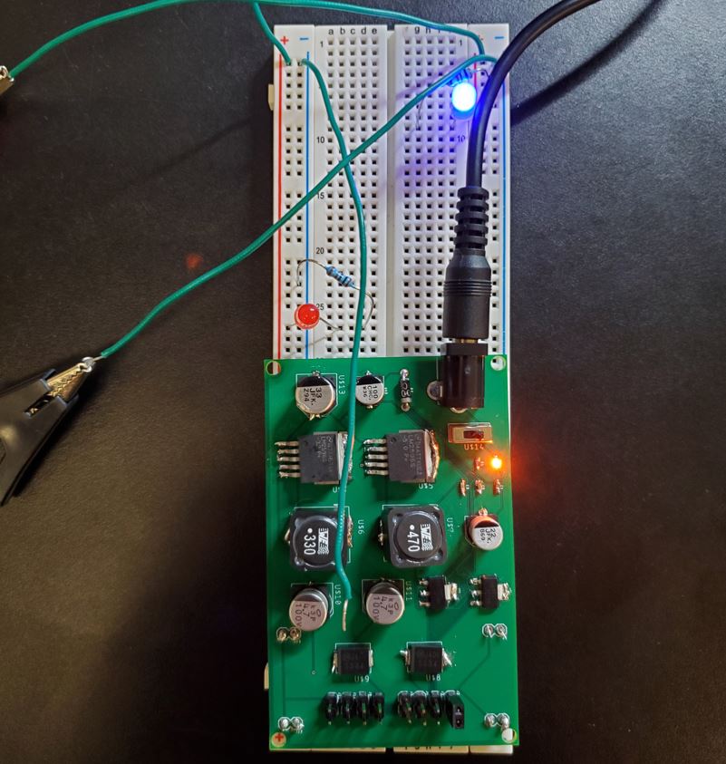
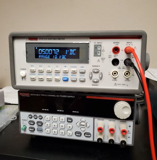
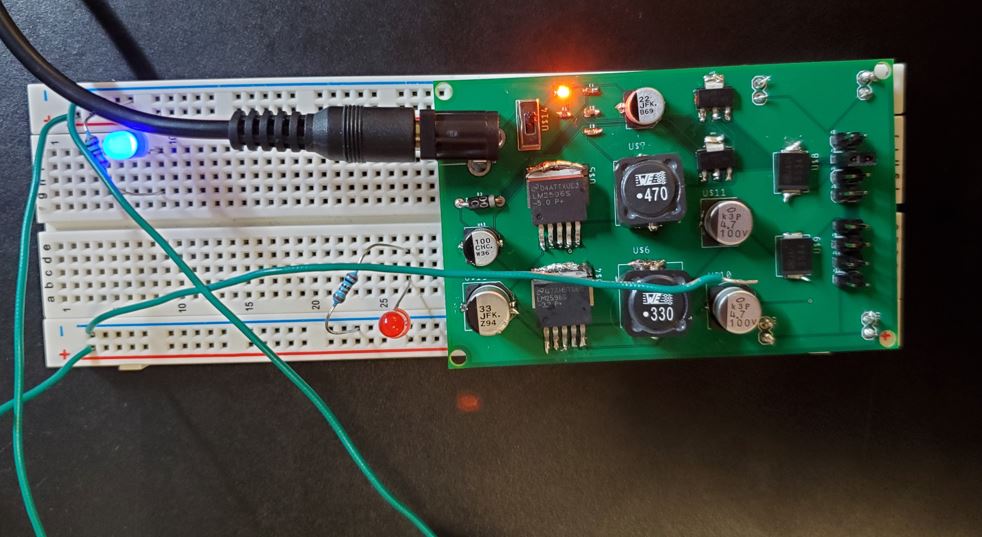
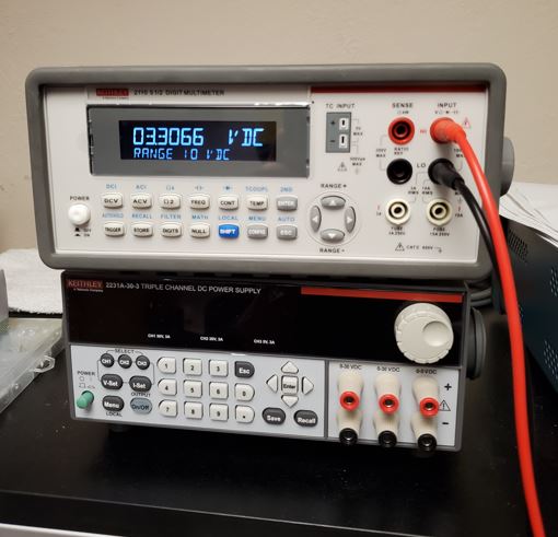
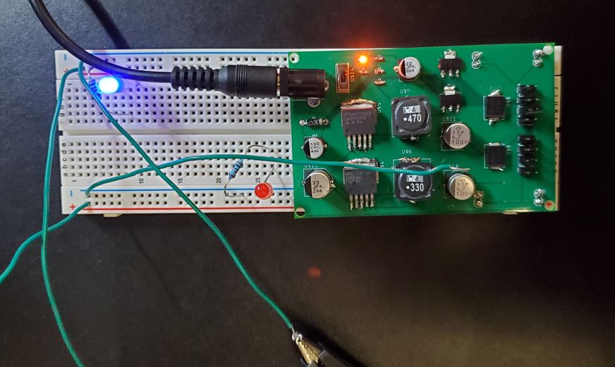
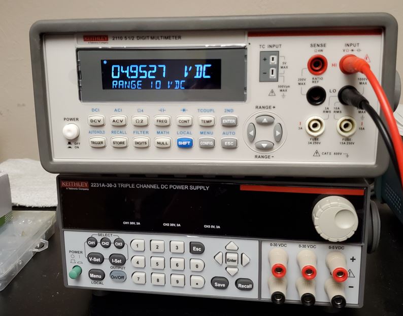
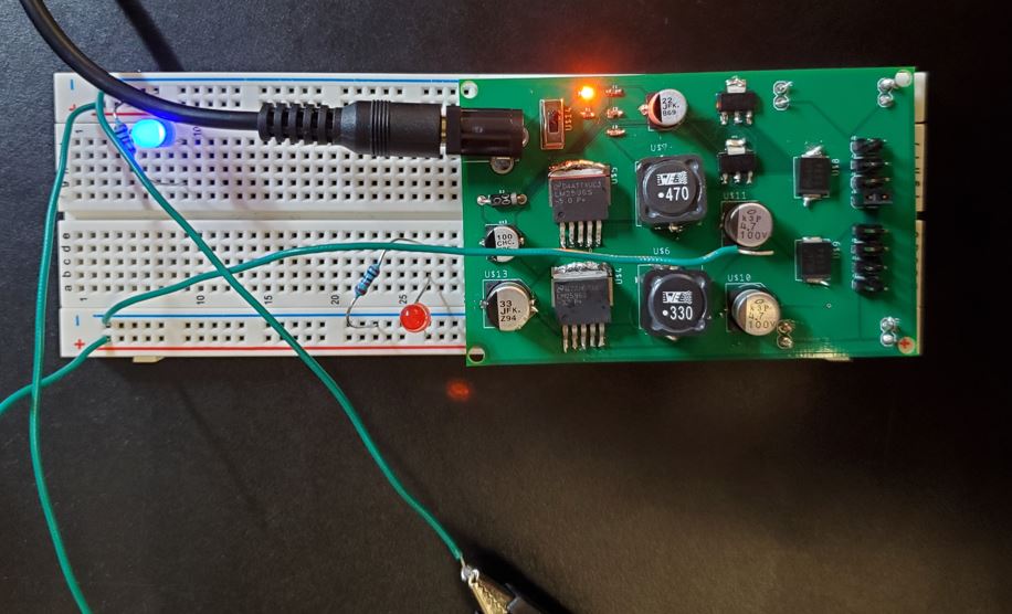
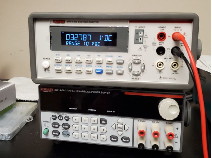
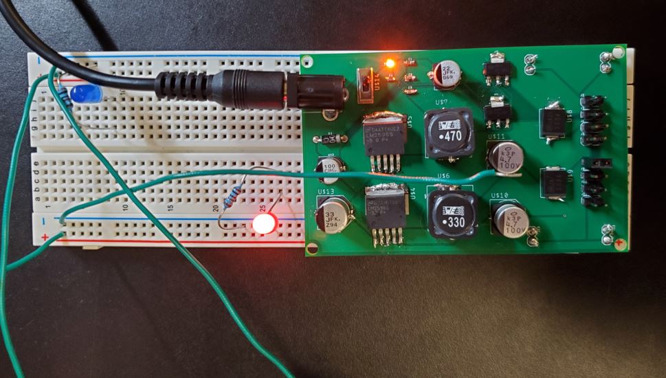
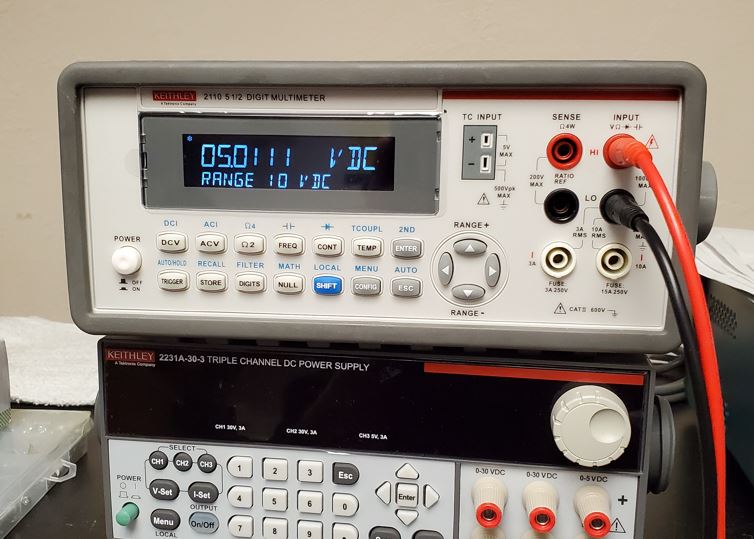
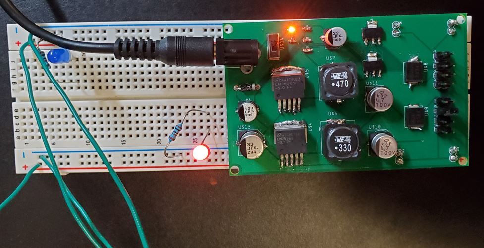
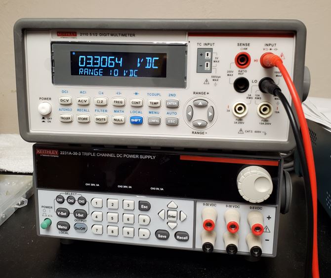
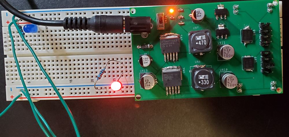
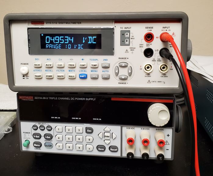
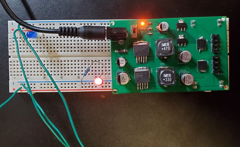
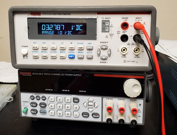
Figure 3-19. (below)
Verification of opperational power distrobution board shown using led
lights and multimeter to test voltages accross terminals. Verification
of each pin starting from far right to left pins 1-8.
5.
Discussion
The applications of soldering all components to create a functional
PCB helped to reinforce previously learned knowledge of PCB design. The
hands on application and the final PCB was impressive and it was nice
to hold what was designed using EAGLE. Soldering can be challenging
sometimes and takes presision and finesse.