1. Using Buses in ElectricVLSI 2. The purpose of this
lab is to build and simulate a ring osillator, design aan 8-bit AND
gate, design an 8-bit OR gate, design an 8-bit NAND gate, and design an 8-bit NOR gate
3. Materials and Methods
LTSpice computer Application
Paper and Pencil
Electric VLSI Application
4. Results
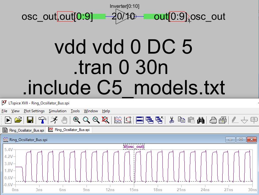
Figure 1. Ring ocsillator schematic simulated using spice code and a 20/10 inverter.
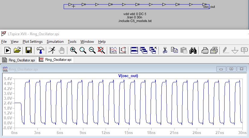
Figure 2. Ring ocsillator using multiple replicated inverters simulated using spice code and a 20/10 inverter.
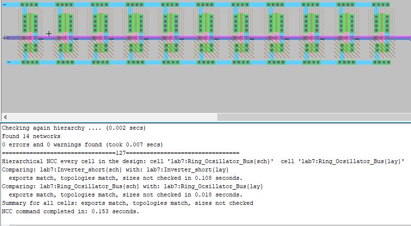
Figure 3. Ring ocsillator layout constructed shown with clean NCC and DRC.
Figure 4. AND gate schematic and simulation shown using Vdd.
Figure 5. AND gate schematic and simulation shown using gnd.
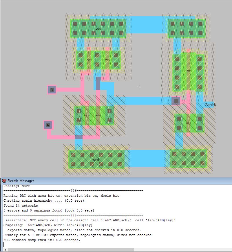
Figure 6. AND gate layout constructed shown with clean NCC and DRC.
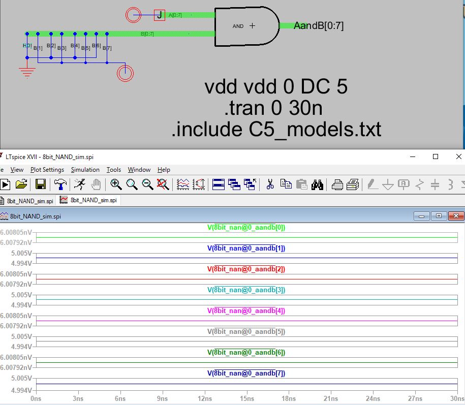
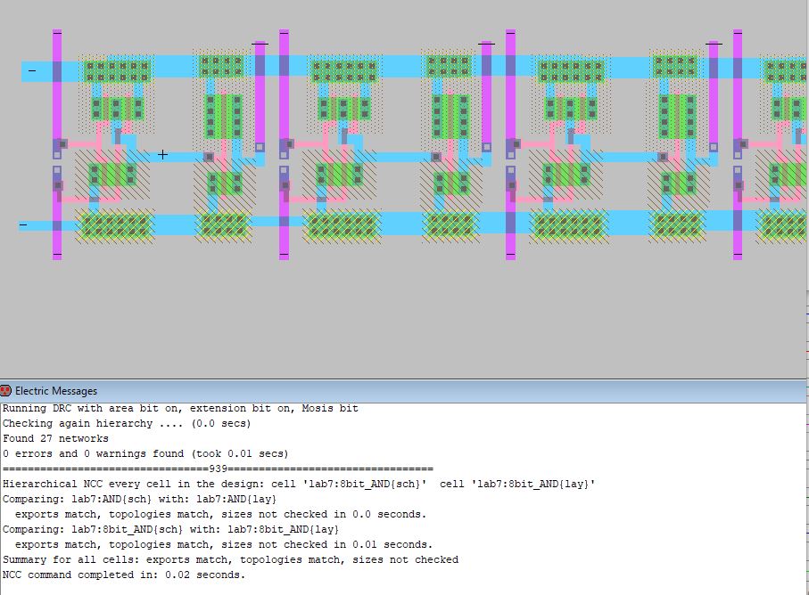
Figure 7. 8 bit AND gate layout constructed shown with clean NCC and DRC.
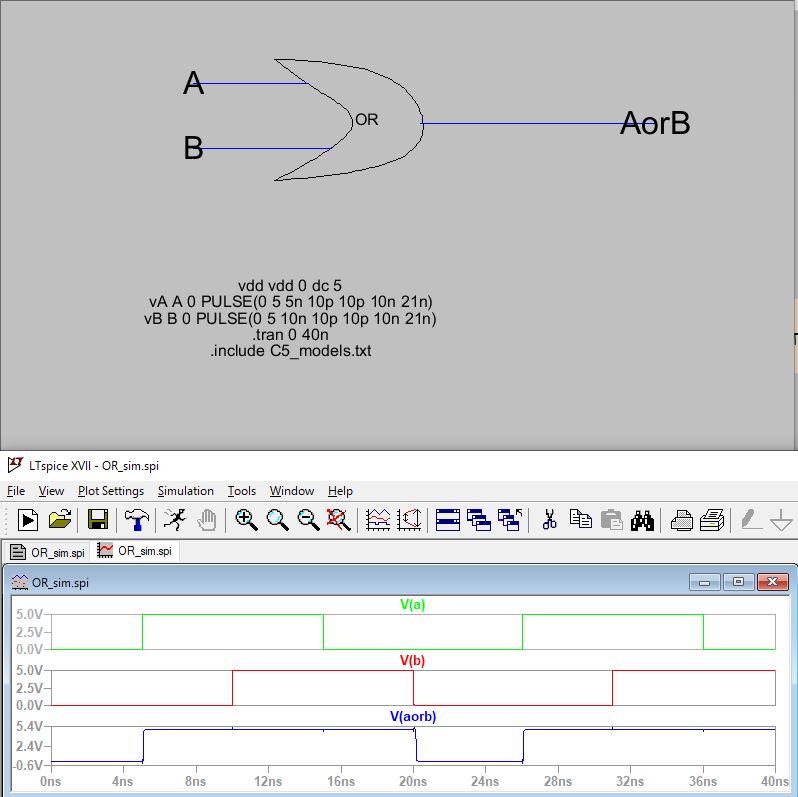
Figure 8. OR gate simulation shown to verify logic before constructing 8 bit.
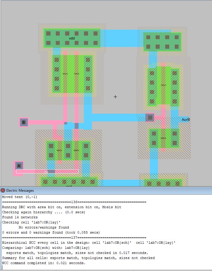
Figure 9. OR gate layout constructed shown with clean NCC and DRC.
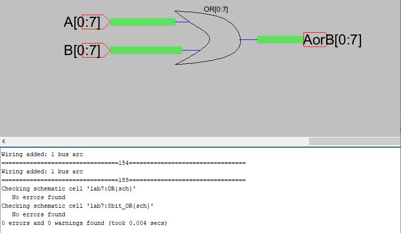
Figure 10. 8 bit OR gate schematic constructed shown with clean DRC.
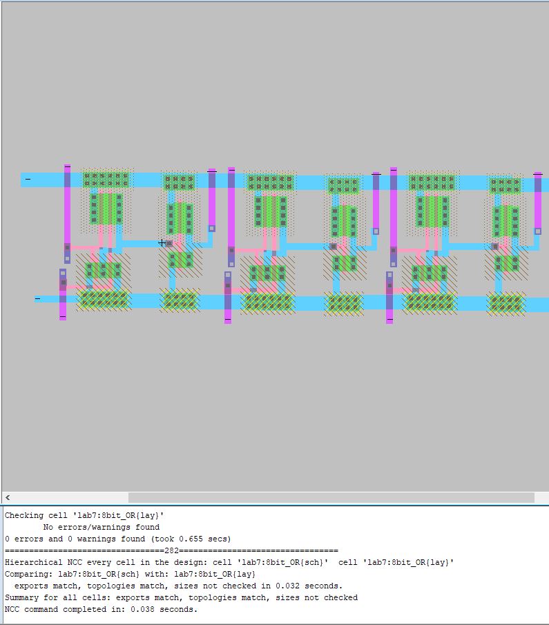
Figure 11. 8 bit OR gate layout constructed shown with clean NCC and DRC.
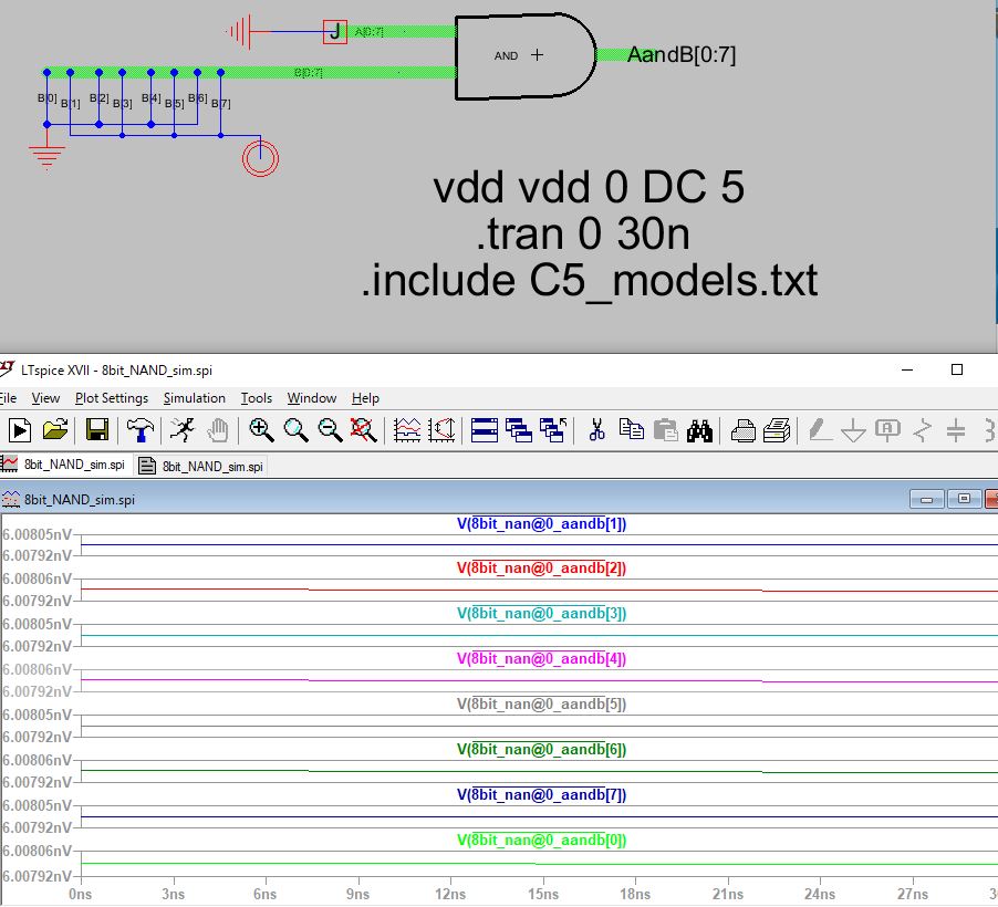
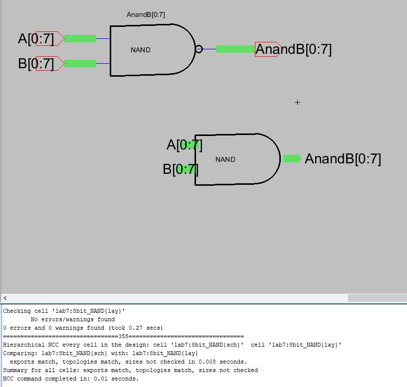
Figure 12. 8 bit NAND gate schematic constructed shown with clean DRC.
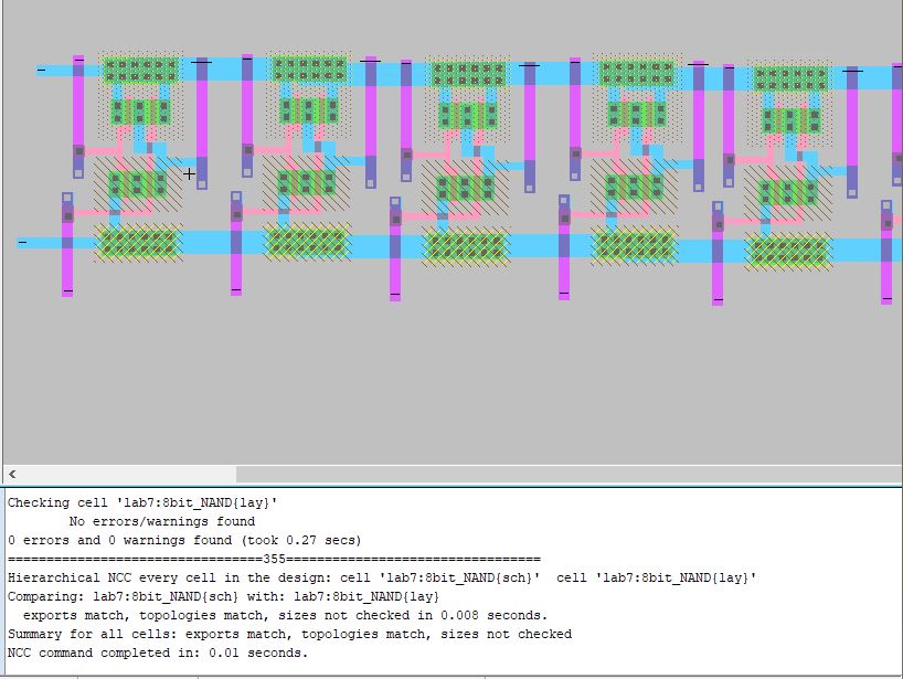
Figure 13. 8 bit NAND gate layout constructed shown with clean NCC and DRC.
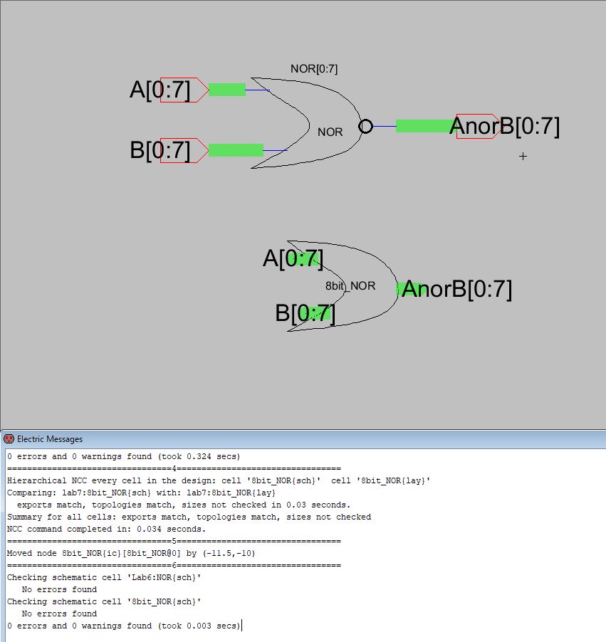
Figure 14. 8 bit NOR gate schematic constructed shown with clean DRC.
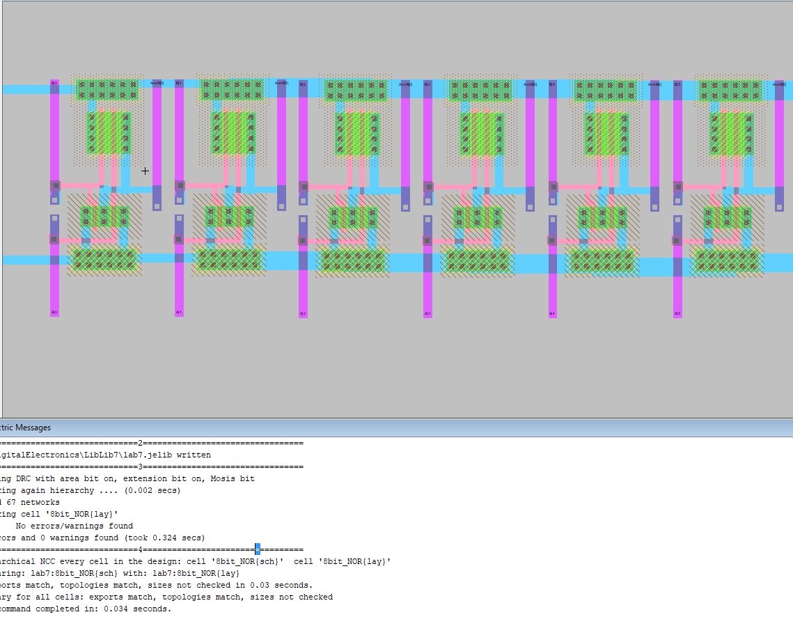
Figure 15. 8 bit NOR gate layout constructed shown with clean NCC and DRC.
5. Discussion
Electric helps to easily replicate singular components and turn
them in to 8 bit or even bigger components. One can observe all the
steps in creating NOR or NAND logic and replicate with ease while
verifying NCC and DRC. It can be for scene that these components will
become important in for future large constructions.