1. The Inverter 2. The purpose of the lab was to construct and inverter using PMOS
and NMOS components. The inverter constucted was also replicated on a
larger scale using the multiplier function in Electric. These inverter
schematics were then simulated using LTSpice software directly paired
with Electric.
3. Materials and Methods
LTSpice computer Application
Paper and Pencil
Electric VLSI Application
4. Results
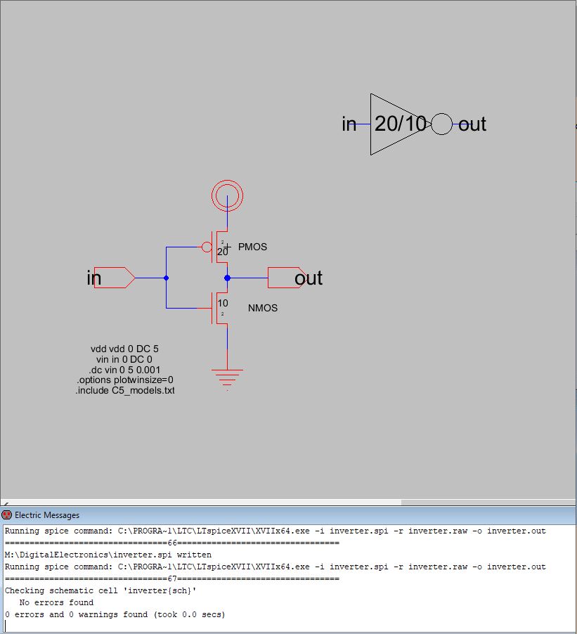
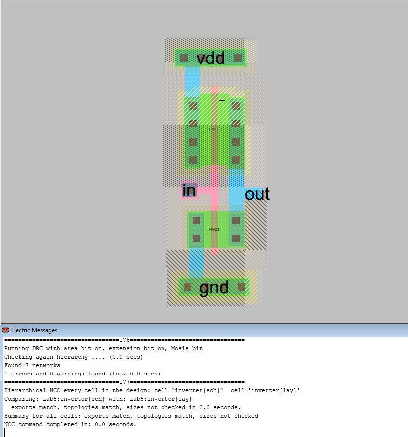
Figure 1. Inverter schematic shown with NMOS and PMOS components and a clean DRC.
Figure
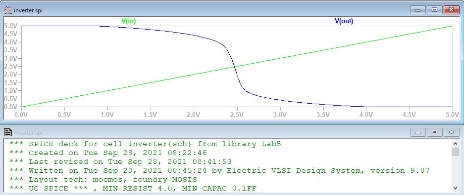
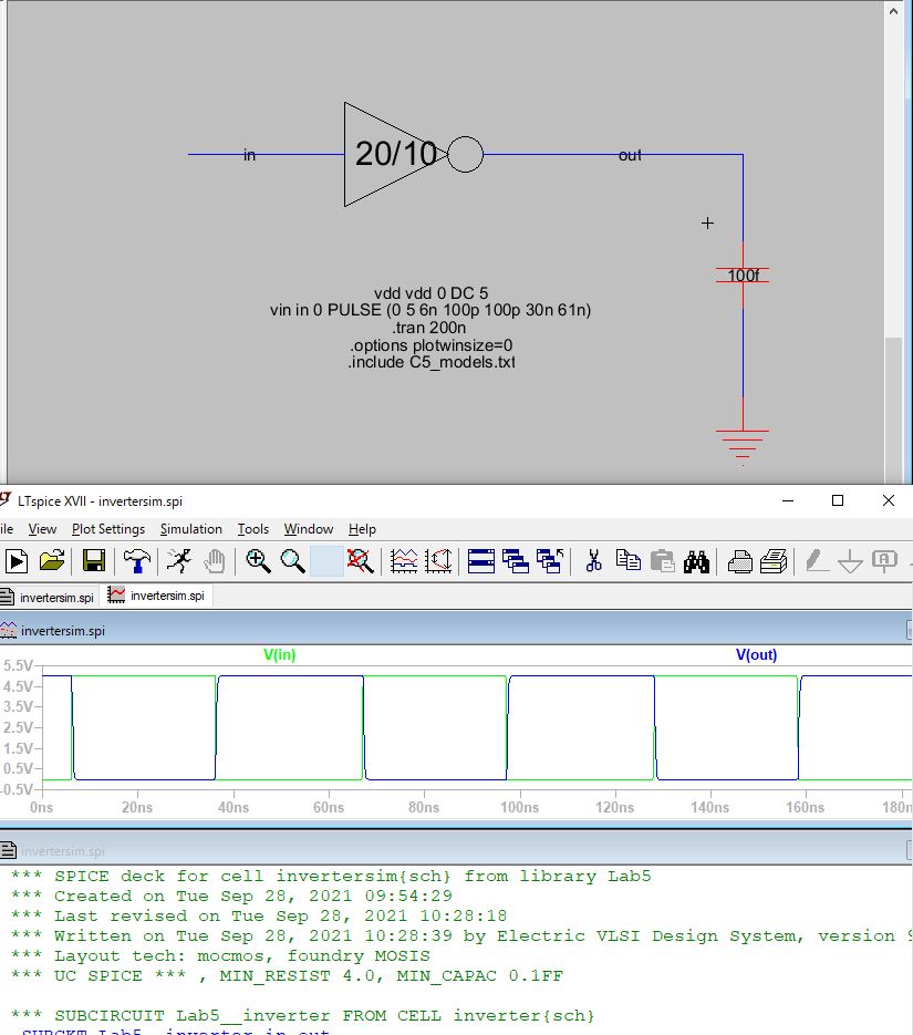
2. Inverter simulation shown where it is clear that the voltage input is an inverted voltage output.
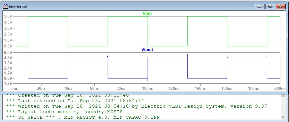
Figure 3. Simulation of the inverter schematic using a pulse function showing the voltage out becomes inverted.
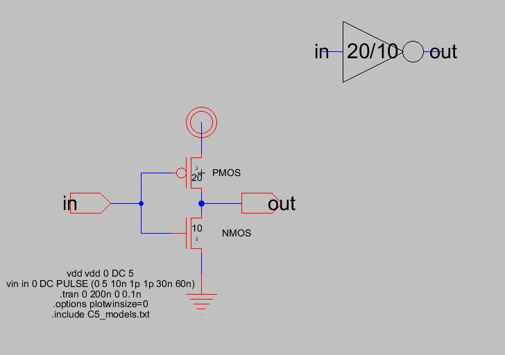
Figure 4. Icon view and schematic view shown of inverter and pulse spice code.
Figure 5. Layout view given of the inverter using NMOS components and PMOS components shown with DRC clean and clean NCC.
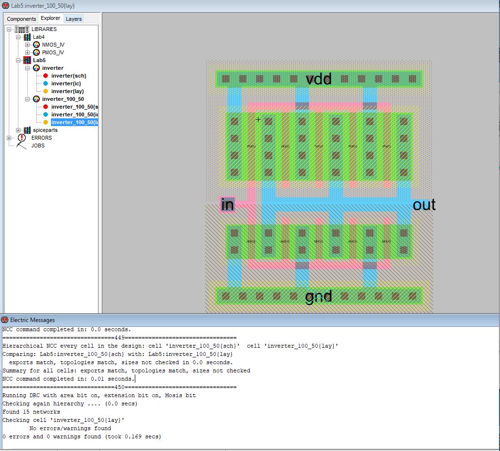
Figure 6. Modified larger inverter of 100/2 and 50/2 shown using replicated PMOS and NMOS components connected together.
Figure 7. Simulation and schematic shown of 20/10 inverter using a 100f capacitor connected to ground.
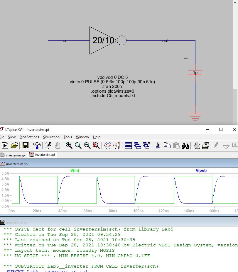
Figure 8. Simulation and schematic shown of 20/10 inverter using a 1p capacitor connected to ground.
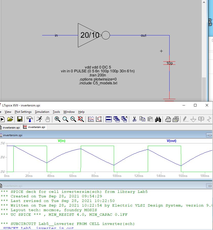
Figure 9. Simulation and schematic shown of 20/10 inverter using a 10p capacitor connected to ground.
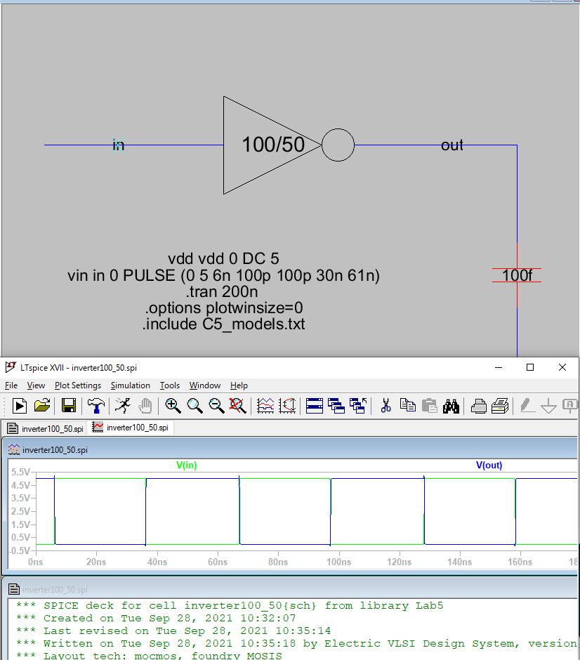
Figure 10. Simulation and schematic shown of 100/50 inverter using a 100f capacitor connected to ground.
Figure 11. Simulation and schematic shown of 100/50 inverter using a 1p capacitor connected to ground.
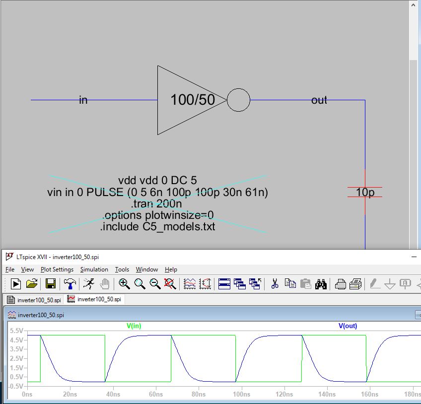
Figure 12. Simulation and schematic shown of 100/50 inverter using a 10p capacitor connected to ground. 5. Discussion
The simulations of the inverters helped to show how the voltage out
is being modified through a circuit. The individual components of the
inverter such as the PMOS and NMOS can be increased in repotition to
create a larger inverter. When there is a larger inverter in allows
more current to flow through the channel. When there is a smaller
inverter less current flows which can take alot of time to fill a
capacitor compared to a large inverter. When the voltage is being
toggled the inverter pulls voltage to the ground or to vdd which is why
the voltage output falls and rises.