Zynq-7000 - Tutorial for PS and PL interconnect in ZedBoard
The
Zynq-7000 SoC integrates the software programmability of an ARM-based
processor with the hardware programmablility of an FPGA. The ZedBoard
from Digilent is part of the Zynq-7000 family which contains a
Dual-Core Cortex-A9 processor and 7-series programmable logic. These
features make the ZedBoard a powerful tool in creating hybrid software
and hardware programmable designs.
This tutorial will
demonstrate the interconnect of ARM processing system (PS) of the
ZedBoard with the FPGA, also known as the programmable logic (PL). To
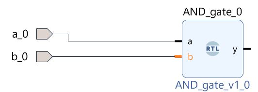
do this, we will model a NAND gate, where the AND logic of the gate is
programmed into the PL and the NOT logic is programmed into the PS. The
inputs will be switches and output will be an LED.
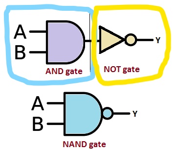
Figure 1: NAND gate schematic. Blue circle will be programmed into the PL and yellow circle will be programmed into the PS.
Materials: ZedBoard kit, ZedBoard constraint file, Vivado Design Suite
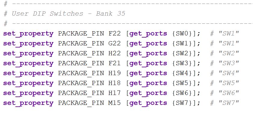
- The constraint file for the ZedBoard can be found here
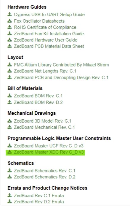
Figure 2: The ZedBoard constraint file needed from Avnet's website.
In your Xilinx folder, create a folder named "Projects" and save the constraint file there.
Step 1: Create a new project!
Open
Vivado and click "Create Project". Title the project NAND_gate and make
sure it is saved to the "Projects" folder as seen below in Figure 3.
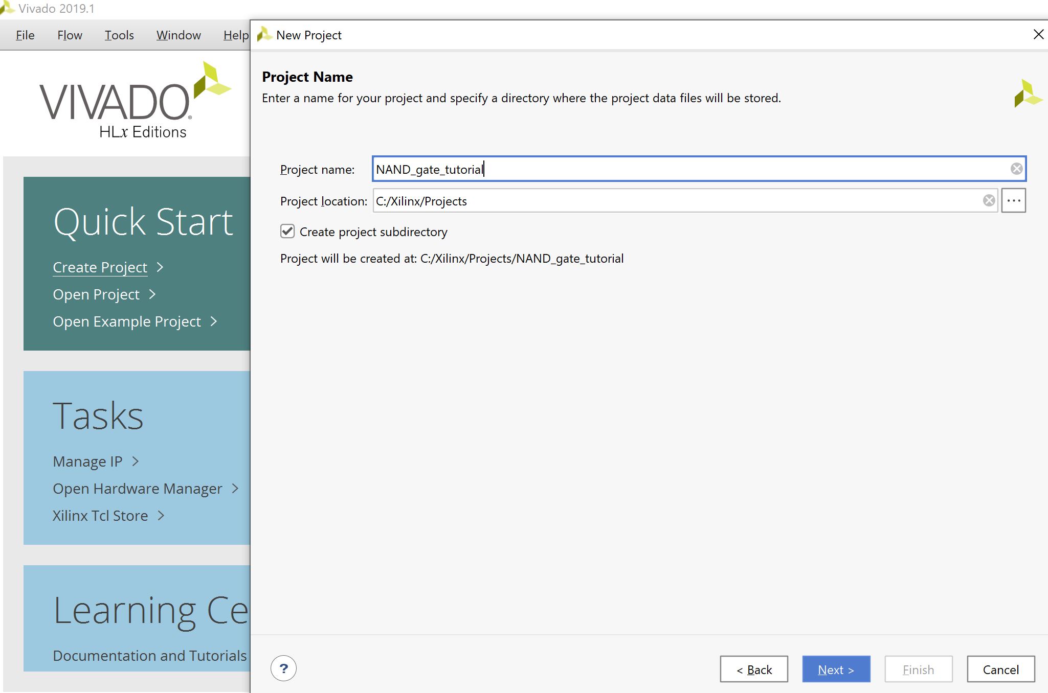
Figure
3: Creating the NAND gate project. Be sure the project is saved inside
the hierarchy of the Xilinx folder. This will be crucial later.
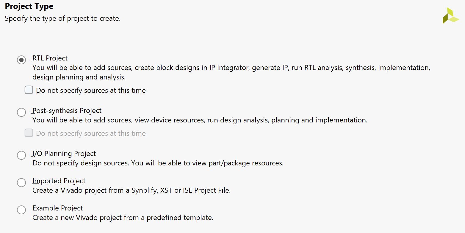
Click Next and make sure RTL project is selected as seen below.
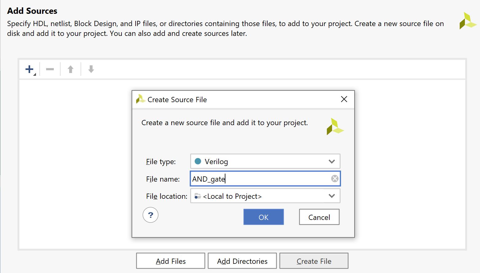
Click
Next again. On the "Add Sources" screen, click create file. This will
be the verilog file that contains that AND gate logic of our NAND gate.
Label it "AND_gate" as seen below and click "Ok" to add it too the
project.
Click
Next again. On the "Add Constraints" page, click add files. Add the
ZedBoard constraint file that was downloaded earlier as seen below. The
constraint file holds the current assigments for all the pins on
the ZedBoard. This allows us to utilize the I/O devices on the ZedBoard.

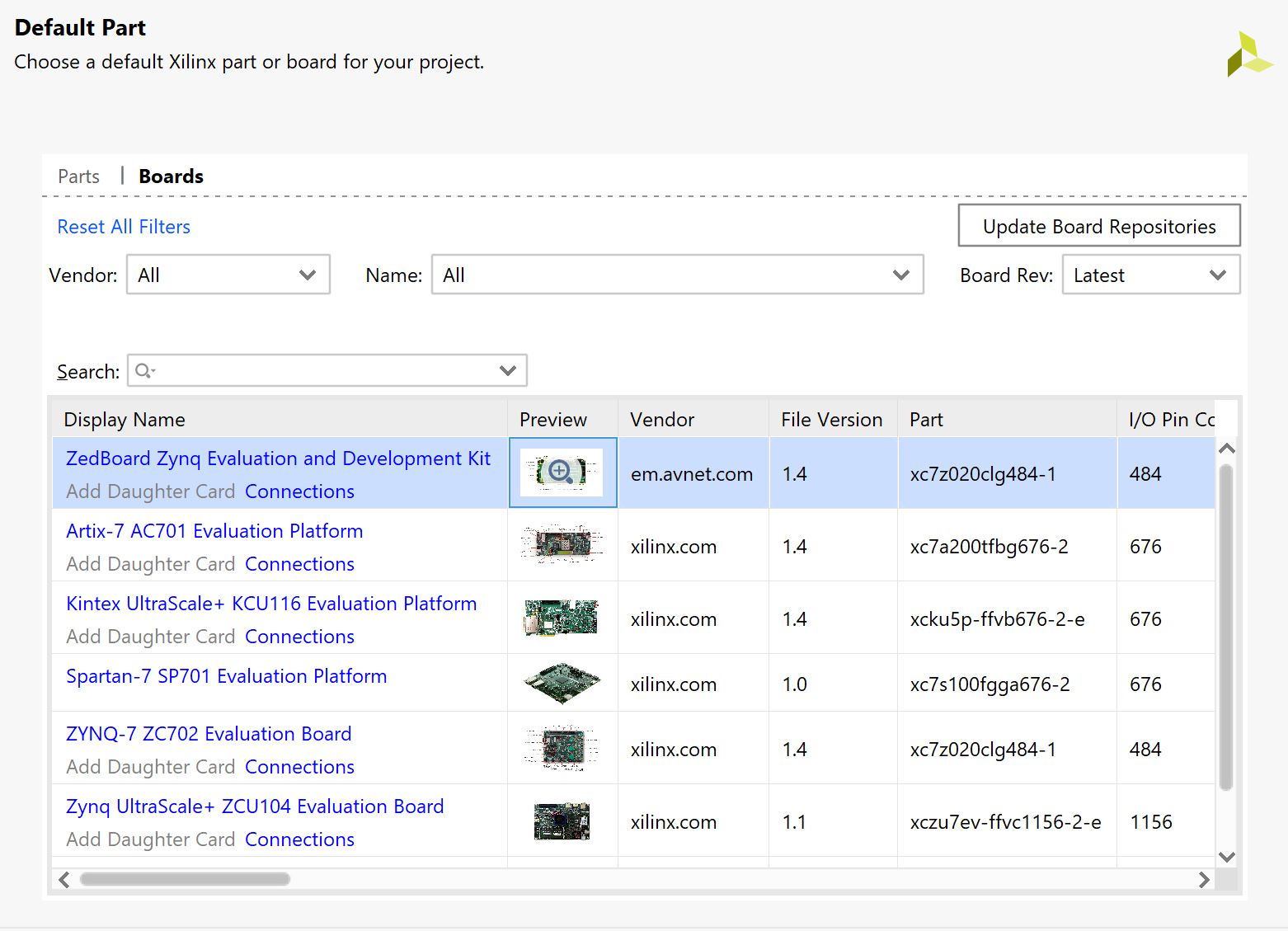
Click Next once again and you will be on the add parts page. Click the boards tab that is highlighted below.
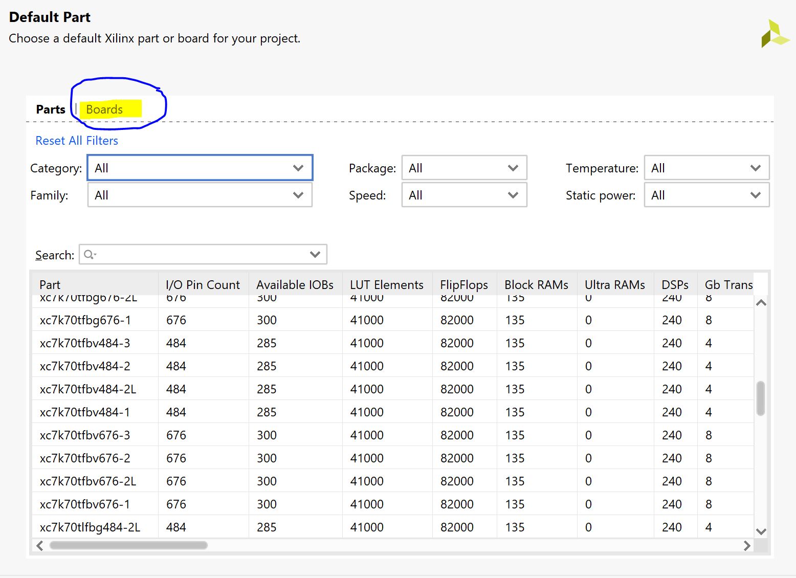
The
boards tab will show all boards one can use for a project. Search
ZedBoard and select the one in blue below. If you cannot find the
ZedBoard, click "Update Board Repositories" and Vivado will download
the latest boards. ZedBoard should be included in those.
Click Next one more time and Vivado should display the screen shown below.
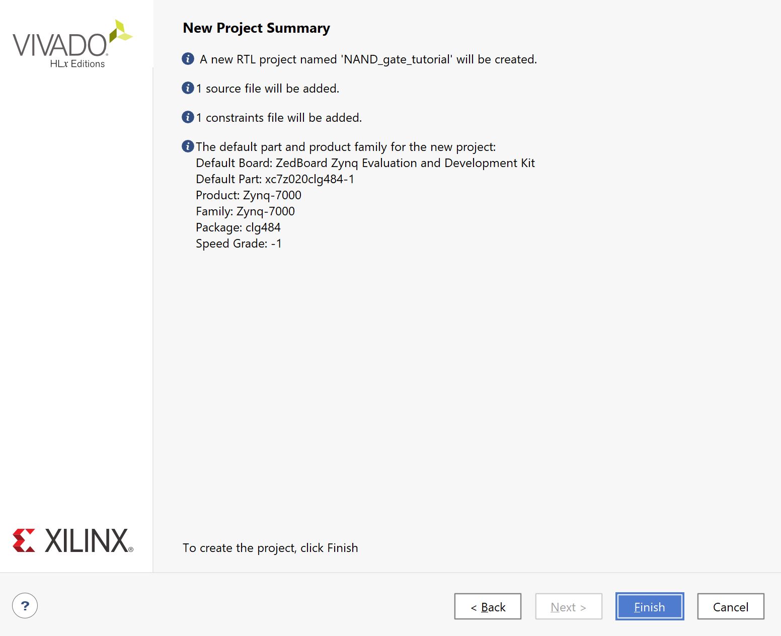
Click
"Finish" and Vivado will create the project for us. When it initially
opens, there will be a few pop-up windows regarding the .v file we
created. Just click 'OK' until you are through to the project.
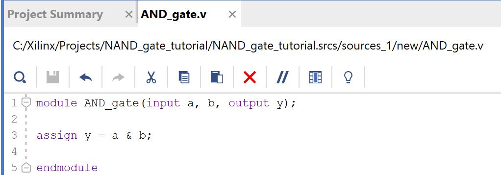
Step 2: Writing the Verilog file
Implement a simple AND gate in the AND_gate.v file we created earlier.
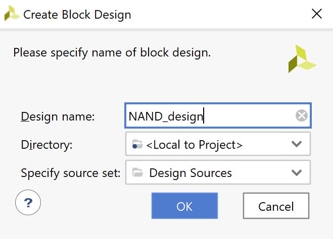
Step 3: Creating the block design
On the Project Manager, click 'Create Block Design', and name it 'NAND_design' as seen below.
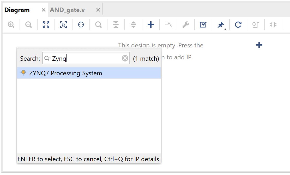
Click
OK to generate the block design, which should be empty. Click the plus
sign and add ZYNQ7's IP block to the design. Double click the IP block
to add.
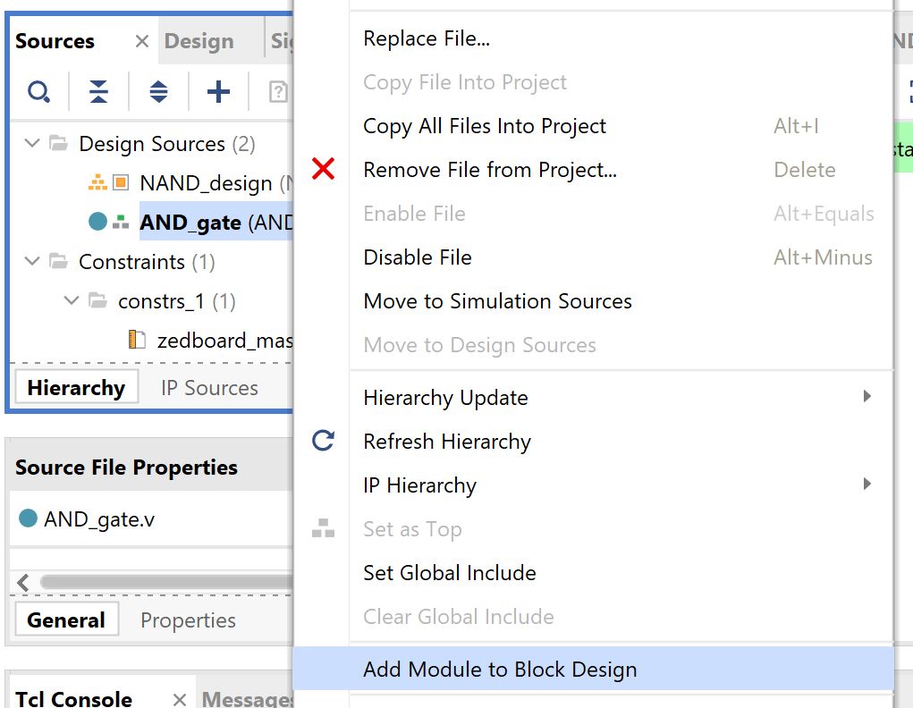
Then, click back to the sources tab, right click on AND_gate.v and select 'Add module to block design'
NAND_design should now look like this:
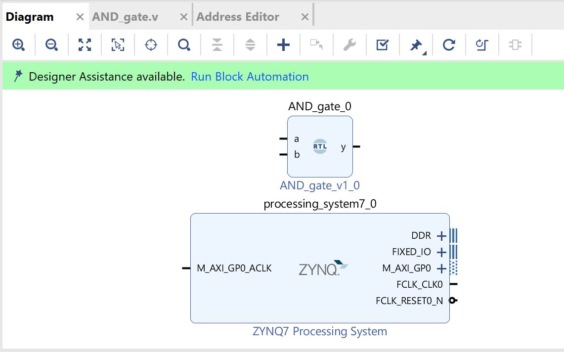
Now
we must instantiate the switches and led. To connect them to the
processing system, we must first instantiate AXI-GPIO blocks. Add two
AXI-GPIO IP blocks to the diagram.
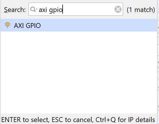
The block diagram should now look like this:
Next,
double click on axi_gpio_0, then click on the IP configuration tab. We
will configure this block to be our inputs via switches. Check the all
input box, then change the GPIO width to be 1, as our inputs will only
be one bit.
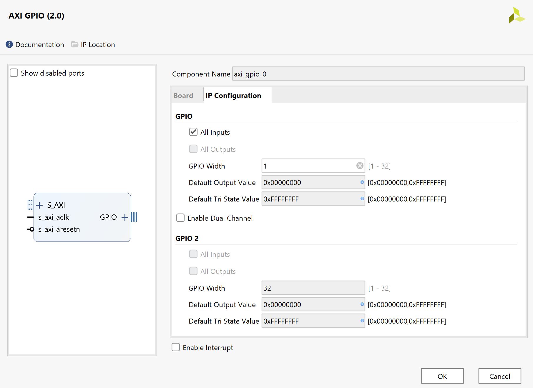
Click
OK. Next, we will instantiate our switches as inputs. Right click the
inputs 'a' and 'b' for our AND_gate module and select make external for
both. (Ctrl T)
This
allows us to make our own inputs for the module. In the constraint
file, the pins for the switches are labeled SW0:SW7 as seen below.
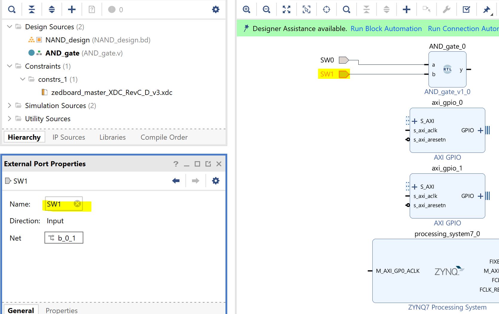
Click
on the external port and in the external port properties window, change
the names a_0 and b_0 to SW0 and SW1. This connects the external ports
to the switches on the board.
Now,
click on the plus sign next to GPIO on the axi_gpio_0 block and
gpio_io_i[0:0] will drop down. Connect our AND gate output y to
gpio_io_i[0:0] by clicking the port and dragging to the other.

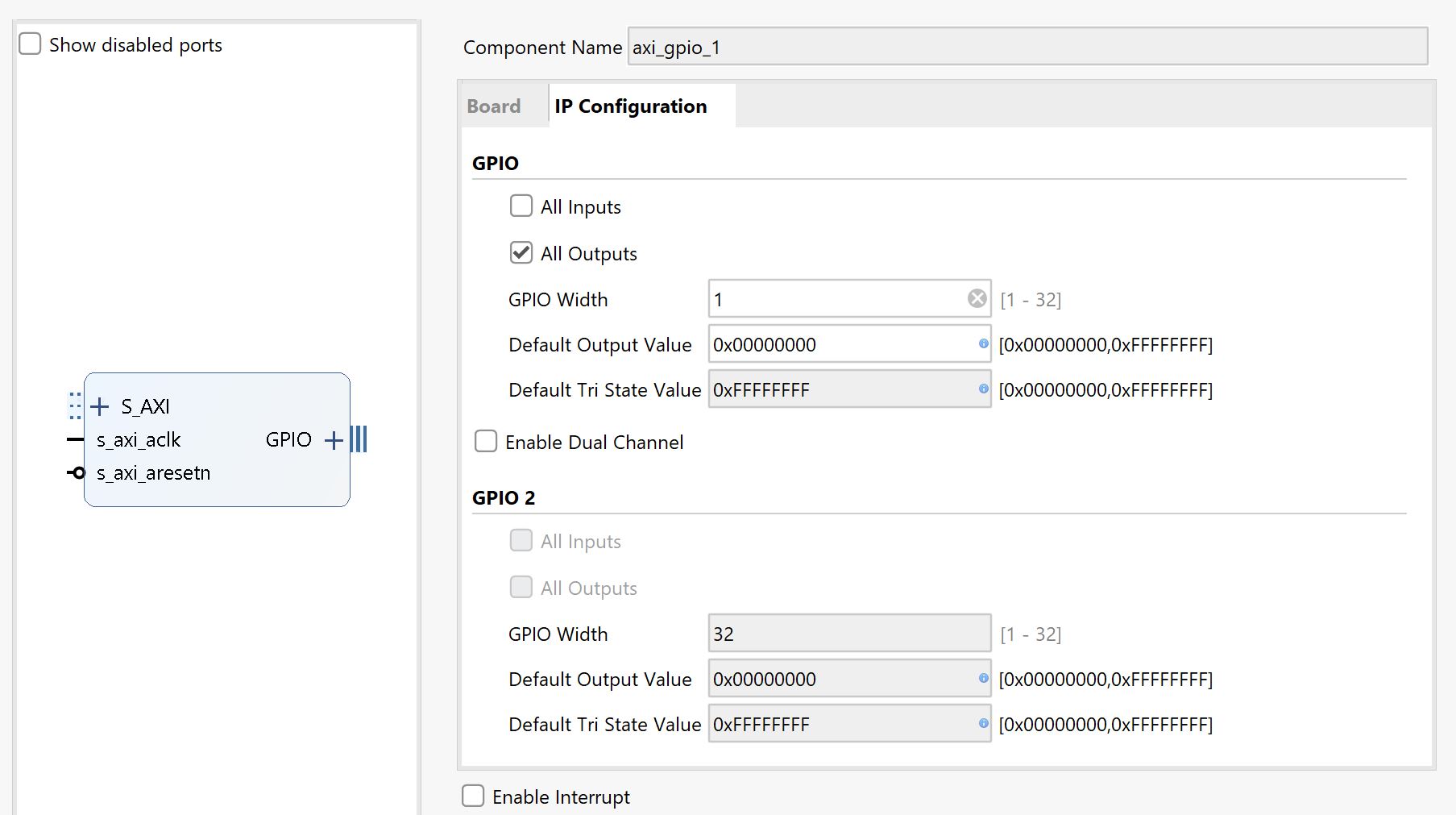
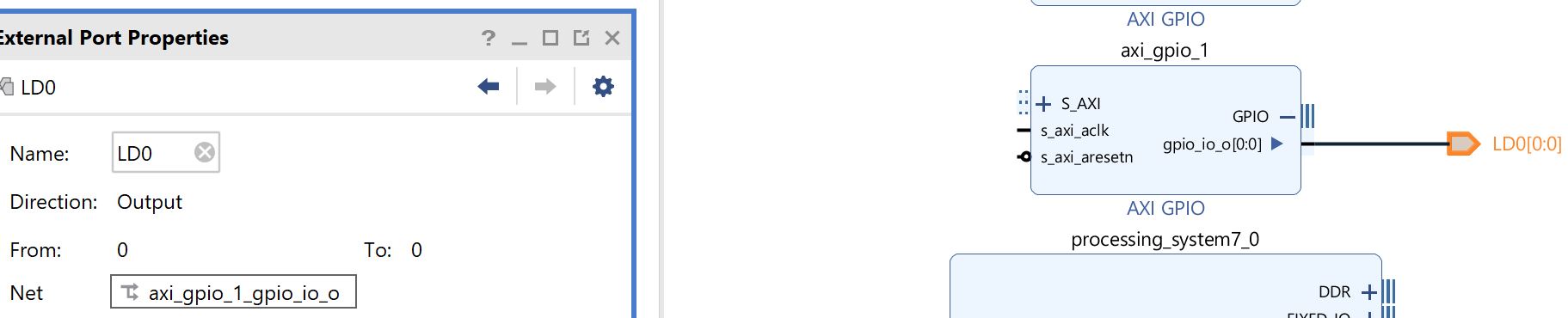
Now,
double click on axi_gpio_1 then move to the IP configuration tab. This
block will serve as an output from the PS to an LED. Check 'All
Outputs' and change GPIO width to 1.
Click
OK. Then, click the plus next to GPIO on the axi_gpio_1 block. Right
click gpio_io_i[0:0] and select make external. (Ctrl T) This will be
our LED. Since LEDs are labeled LD0:LD7 in the constraints file,
we will label this external port LD0 to connect it to the first
LED on the board. Do this in the external port properties
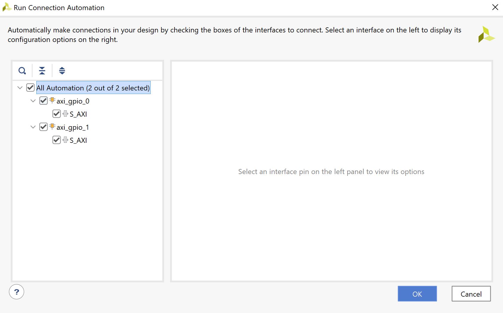
Now, click Run Connection Automation above the block diagram. Select 'All Automation' and hit okay.
After,
click Run Block Automation, then click the clockwise arrow icon that is
highlighted below to regenerate the layout. The block design should now
look like:
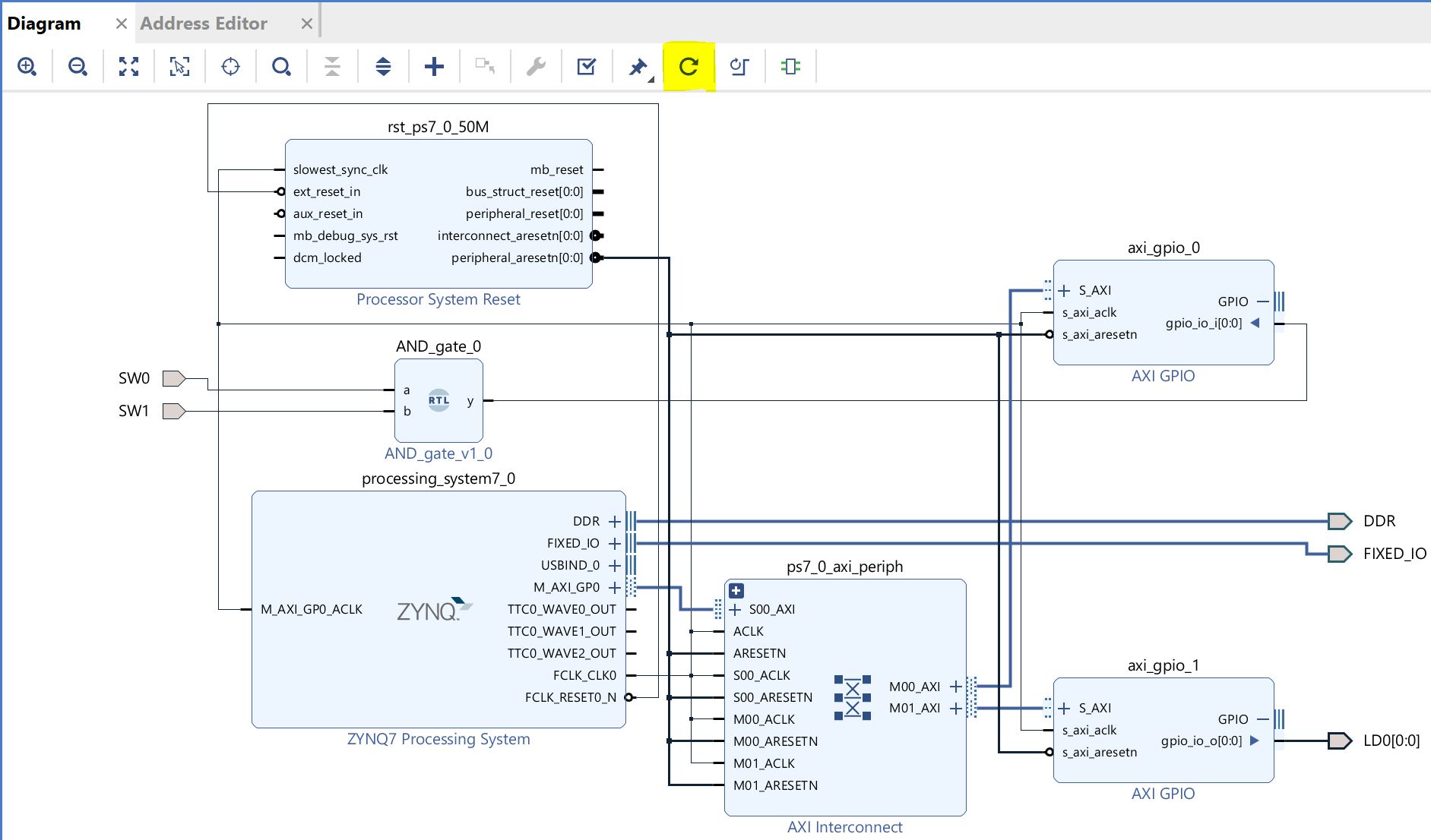
The
axi_peripheral block is added to connect the axi_gpio's to the
processing system. Also a system reset block is added during connection
automation.
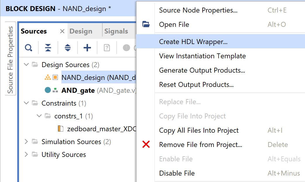
4. Create an HDL wrapper
That is all the hardware design needed. Now, go
back to the sources tab, right click on NAND_design and then click
'Create HDL Wrapper'. Choose 'Let vivado manage wrapper'.
The
HDL wrapper wraps all IP blocks up into one module, which can then be
synthesized, implemented, and written into a bitstream file. On the
bottom left of the flow navigator, click 'Generate Bitstream'. Once
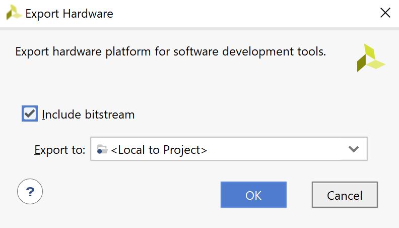
completed, click on file, export, then export hardware. Be sure include
bitstream is selected.

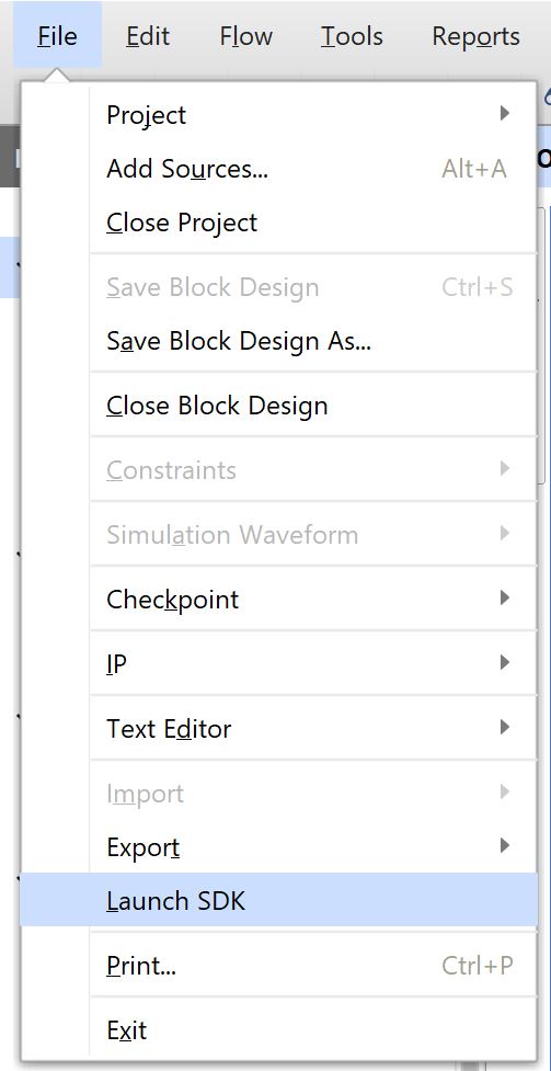
Once exported, click on file again, then Launch SDK. Both options should be local to project.
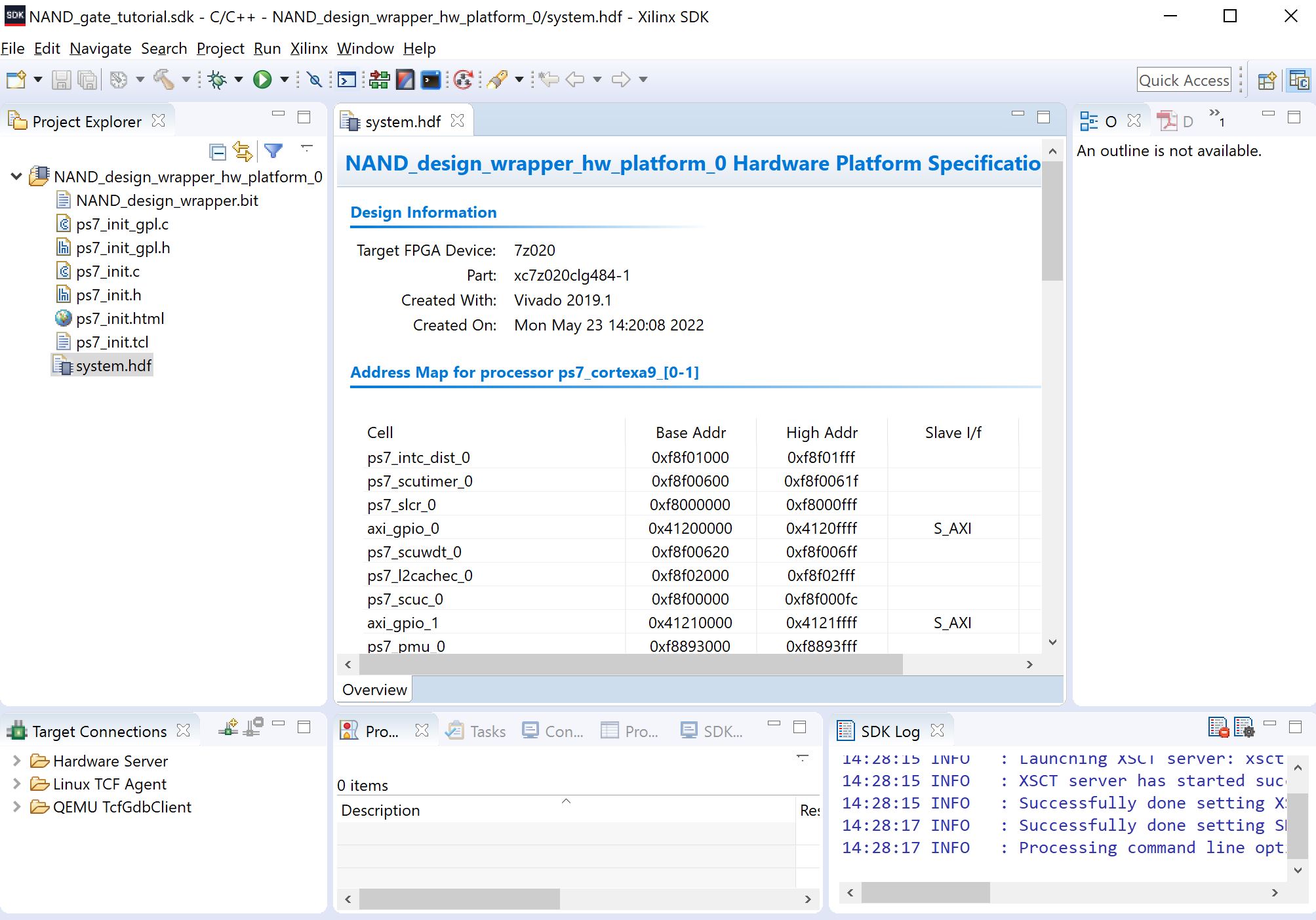
5. Creating a .c file
Don't select anything at first and the hardware wrapper should open in SDK.
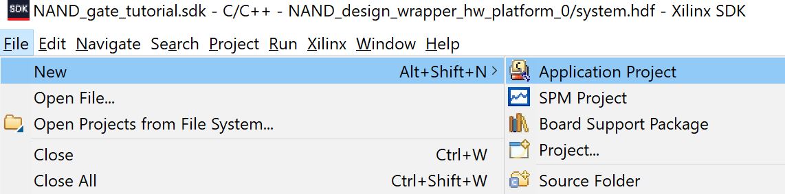
Next, click file - new - application project
Name
the project "NOT_gate" then click next> and make sure the source
file 'helloworld.c' is selected. This will be the template for our .c
file.
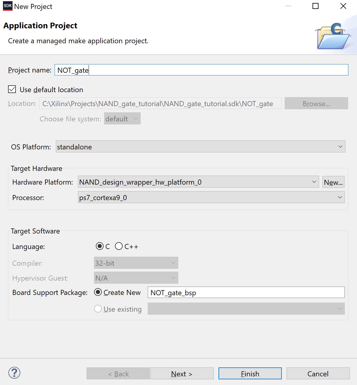
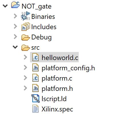
This
will generate a NOT_gate folder. Now, open the NOT_gate folder on the
left, then open the src folder. Then, double click "helloworld.c" to
open the .c file.
Now
we can code up our .c file. First, we initialize XGpio variables named
input and output. We then connect these variables to our AXI_GPIO
blocks in the block design. We do this by using the XGpio_Initialize
function. In our diagram, we designed the AND gate output to be input
through AXI_GPI0_0. So, we initialize the input variable with the
GPIO_0 device ID. We also initialize our output to GPIO_1 device ID as
that block corresponds to our output LED.
After that, we set
the data direction of the two variables accordingly.
XGpio_SetDataDirection(&var, on/off(1/0), input/output(1/0)). Then,
we are able to read data from our inputs using the discrete read
function. Once we read in data from the AND gate, we set it into an
integer a. Next, we invert the data, creating a NOT gate. We are then
able to write the data back to the PL using the discrete write
function.
Full .c code is given below:
/*
2-bit NOT gate to test PL and PS interconnect
*/
#include <stdio.h>
#include "platform.h"
#include "xgpio.h"
#include "xparameters.h"
int main()
{
init_platform();
XGpio input, output;
int a; // input of NOT gate (output of AND gate)
int y; // output of NOT gate (output of NAND gate)
XGpio_Initialize(&input, XPAR_GPIO_0_DEVICE_ID);
XGpio_Initialize(&output, XPAR_GPIO_1_DEVICE_ID);
XGpio_SetDataDirection(&input, 1, 1);
XGpio_SetDataDirection(&output, 1, 0);
while(1)
{
a = XGpio_DiscreteRead(&input, 1);
if(a==1)
{
y = 0;
}
else // a=0
{
y = 1;
}
XGpio_DiscreteWrite(&output, 1, y);
}
cleanup_platform();
return 0;
}
6. Interconnecting the PL and PS
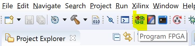
Now
save the file and we are now ready to program the ZedBoard. Make sure
the ZedBoard is plugged in and turned on, then connect it to your
computer through the JTAG port via micro-USB. Next, click program FPGA.
Don't change any settings, click program again to program the PL.
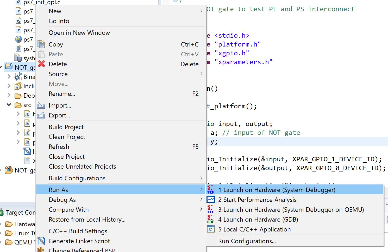
Then,
right click on the NOT_gate folder, click Run As, then Launch on
Hardware (System Debugger) to program the .c file to the PS.
Congratulations,
you have now connected the programmable logic of the ZedBoard to the
ARM processor. We can verify this using the switches. The truth table
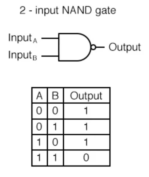
for a 2-bit NAND is as follows:
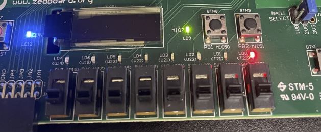
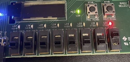
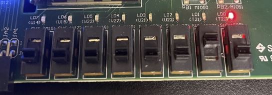
So, the LED should only be turned off when both switches our turned on. Outputs should look identical to the photos below:
These outputs demonstrate a successful interconnect between the programmable logic and the processing system!