ENGR 338 Lab 6 - Build a NAND, NOR, XOR, and Full Adder
Name: Max Krauss
Email: mtkrauss@fortlewis.edu
Introduction: For this two week lab, we built and simulated logic gates and a Full Adder with cmos transistors in Electric VLSI.
Task 1: Create the schematic and layout of the NAND gate. (15 points)
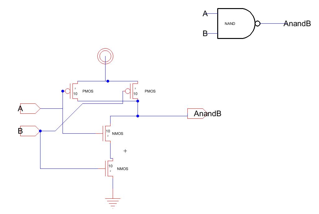
Figure 1: Electric VLSI schematic for the NAND gate.
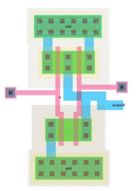
Figure 1.1: Electric VLSI layout for the NAND gate
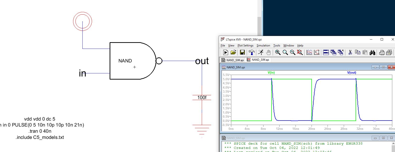
Figure 1.2: Spice simulation of the NAND gate
Task 2: Create the schematic and layout of the NOR gate. (15 points)
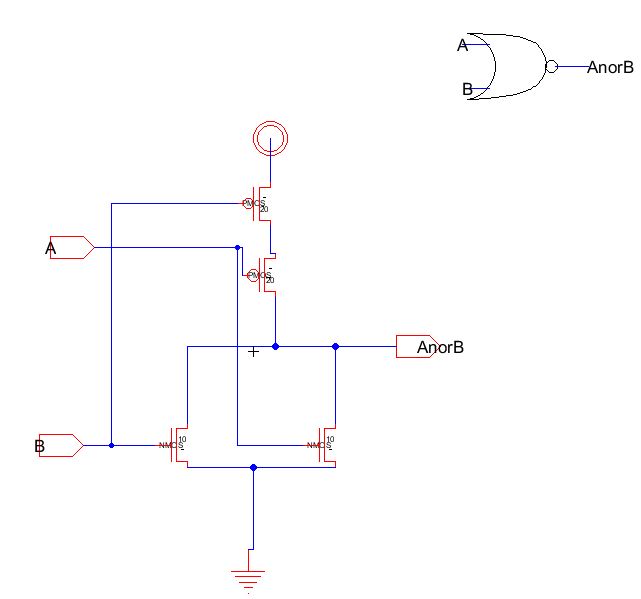
Figure 2: Electric VLSI schematic for the NOR gate
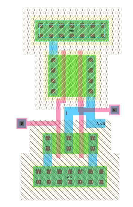
Figure 2.1: Electric VLSI layout for the NOR gate
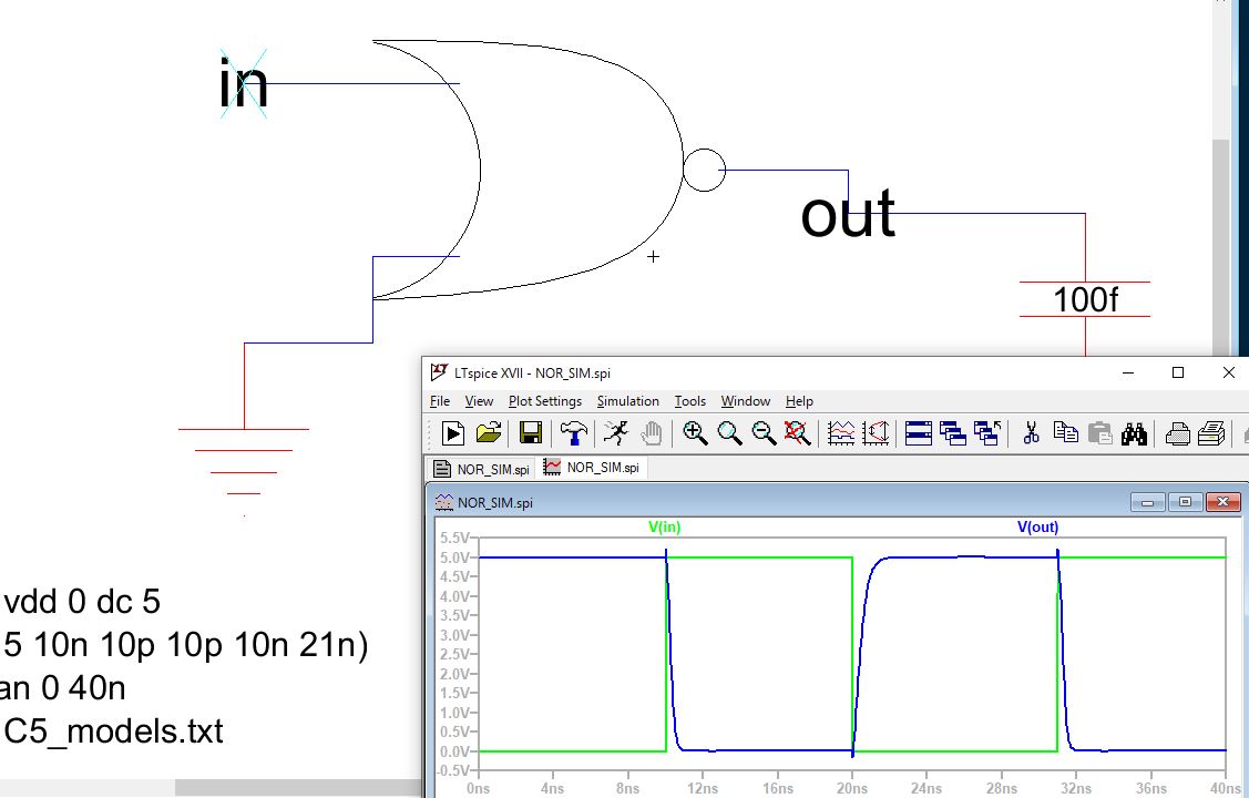
Figure 2.2: Spice simulation of the NOR gate
Task 3: Design, simulte, and layout an XOR gate. (30 points)
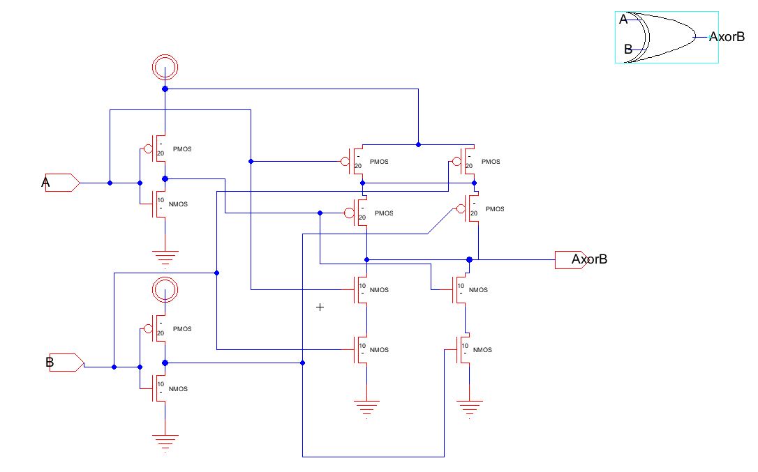
Figure 3: Electric VLSI schematic of the XOR gate
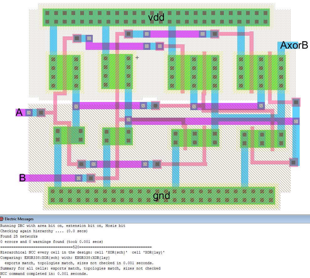
Figure 3.1: Electric VLSI layout of the XOR gate
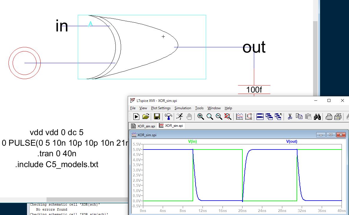
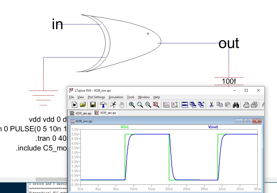
Figure 3.2: Spice simulation for the XOR gate.
Task 4: Design, simulte, and layout an Full Adder. (30 points)
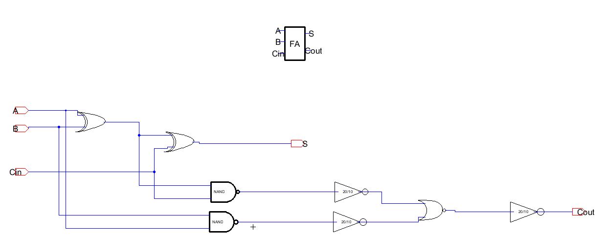
Figure 4: Electric VLSI schematic for the Full Adder
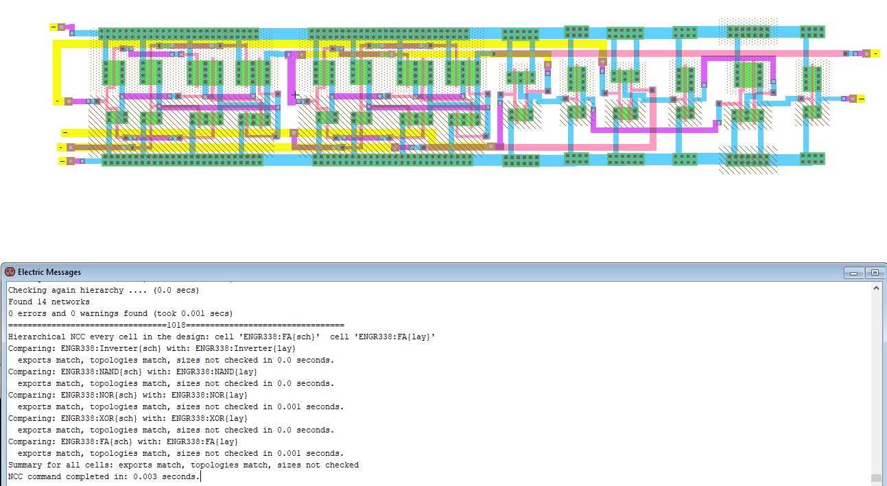
Figure 4.1: Electric VLSI layout for the Full Adder
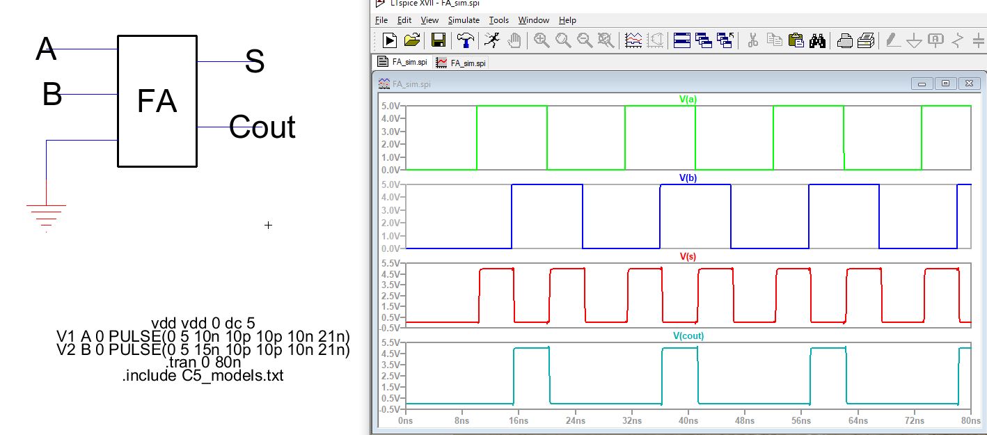
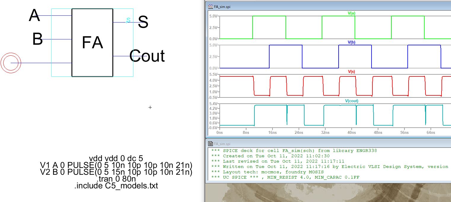
Figure 4.2: Spice simulations for the FA
Conclusion: This lab was a
good resource in learning AOI logic and CMOS gate layouts. The FA
layout took hours, but was satisfying when it finally passed NCC and
DRC.