ENGR 338 - Lab 2
Name: Max Krauss
Email: mtkrauss@fortlewis.edu
Lab 2 - Design an R-2R DAC
Objectives:
1. Understand the operation of the ideal ADC and DAC
2. Design a R-2R DAC in Electric VLSI to replace the ideal DAC
3. Be familiar with Electric VLSI and LTSpice for integrated circuit design
Task 1: Copy the existing ideal ADC-DAC files to your ENGR338 library and run the simulation. (30 points).
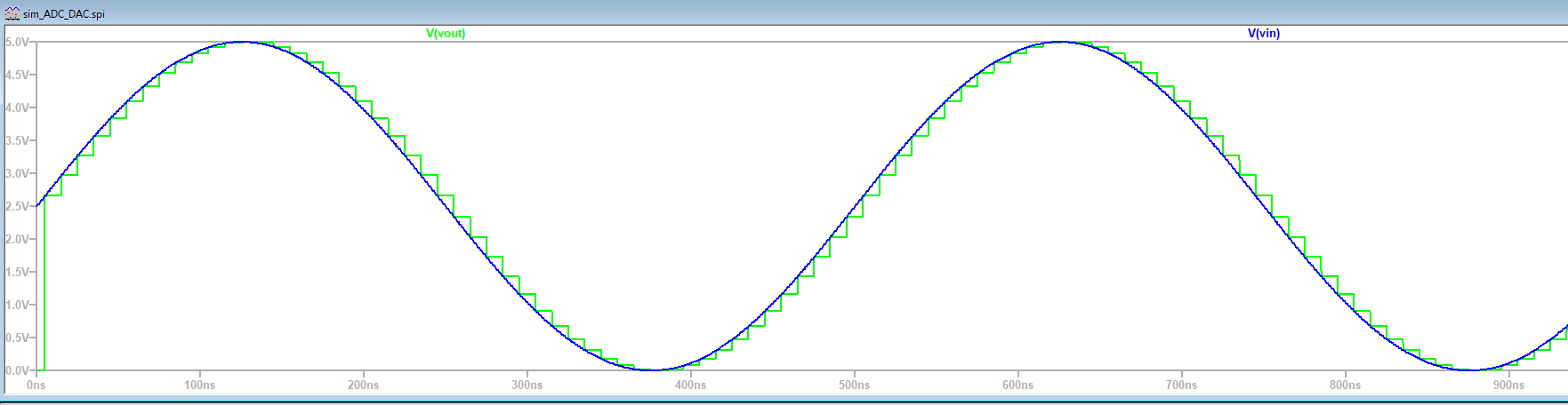
Figure 1: LTSpice simulation of the ideal ADC-DAC from existing files.
Task 2: Build the schematic of the R-2R DAC and run the simulation. (30 points).
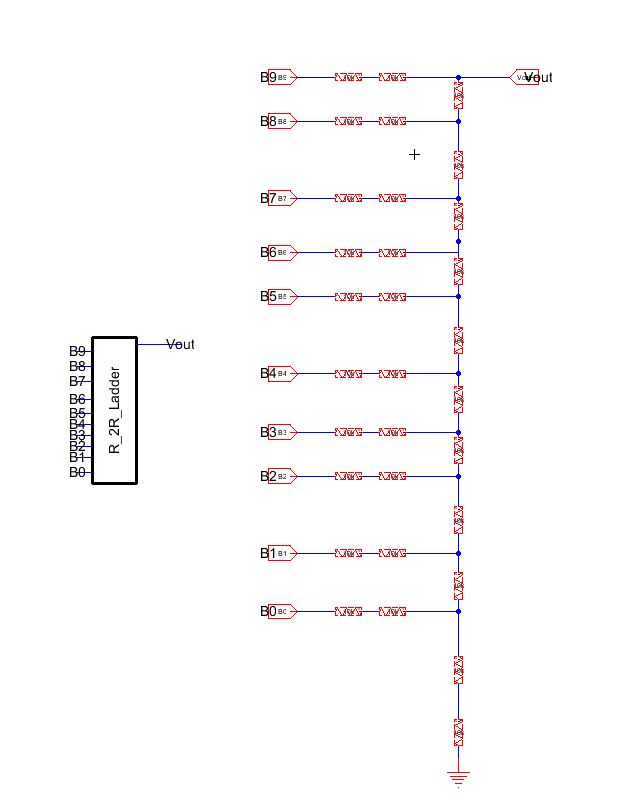
Figure 2: R-2R Ladder Layout in Electric VLSI
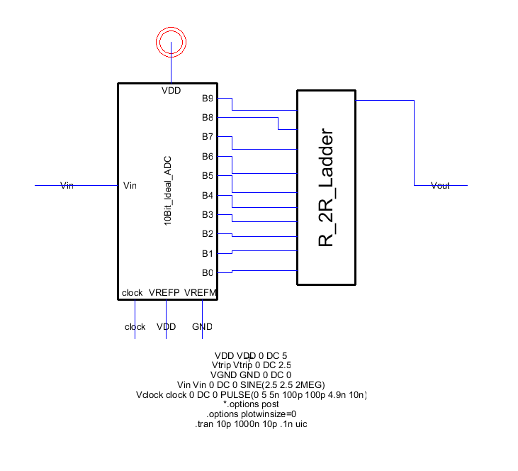
Figure 3: Ideal ADC connected to R-2R Ladder DAC
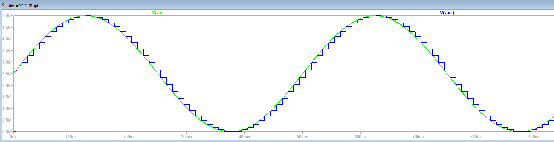
Figure 4: LTSpice simulation from the Ideal ADC R-2R Ladder DAC
Task 3: Test the time delay from the B9 pin when the DAC drives a 10 pF load. (30 points).
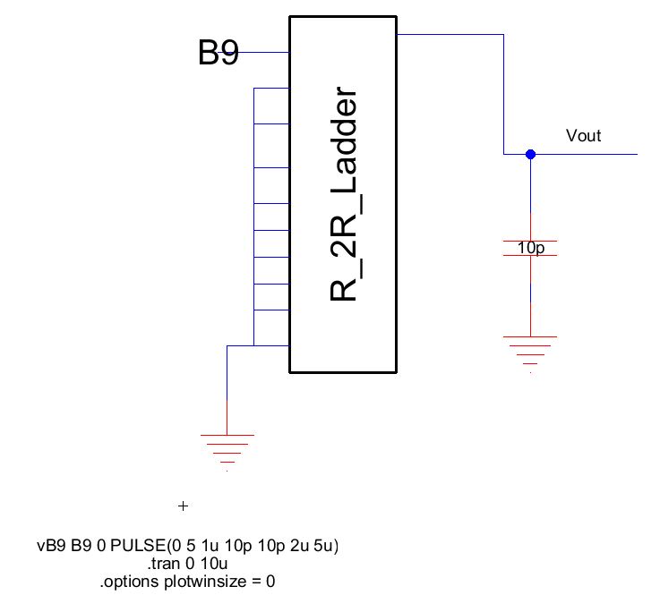
Figure 5: R-2R Ladder DAC w/ all pins but B9 shorted to ground and a 10 pF load
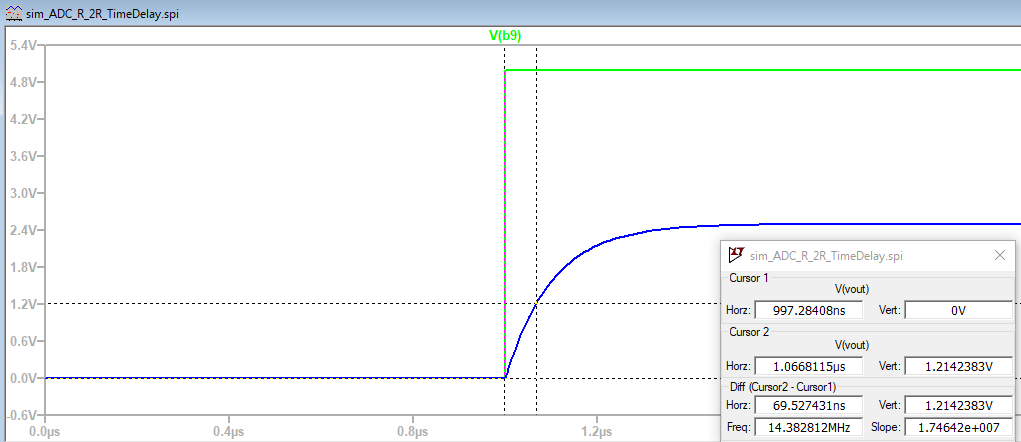
Figure 6: LTSpice simulation demonstrating the time delay for task 3.
Conclusion: This lab was a good intro for the Electric VLSI software.
It also helped us become more familiar with the R-2R DAC layout.