ENGR 338 - Cadence Tutorials 1-2
Name: Max Krauss
Email: mtkrauss@fortlewis.edu
- Tutorial 1 -
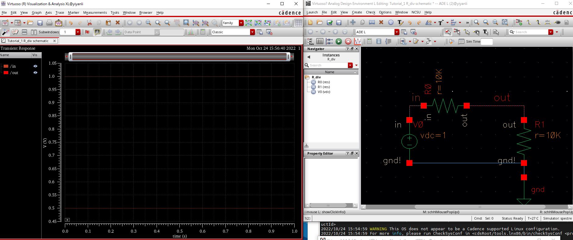
Figure 1: Schematic simulation of a voltage divider.
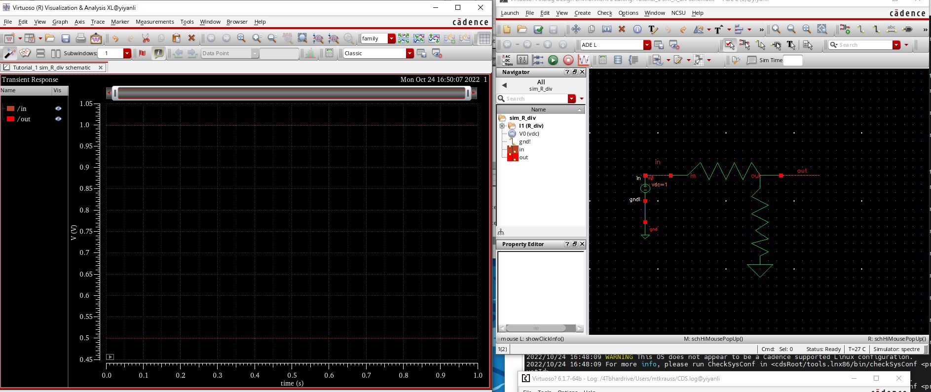
Figure 2: Symbol simulation of a voltage divider.
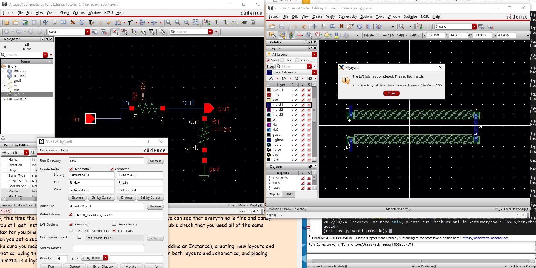
Figure 3: Layout of voltage divider which completed LVS check.
- Tutorial 2 -
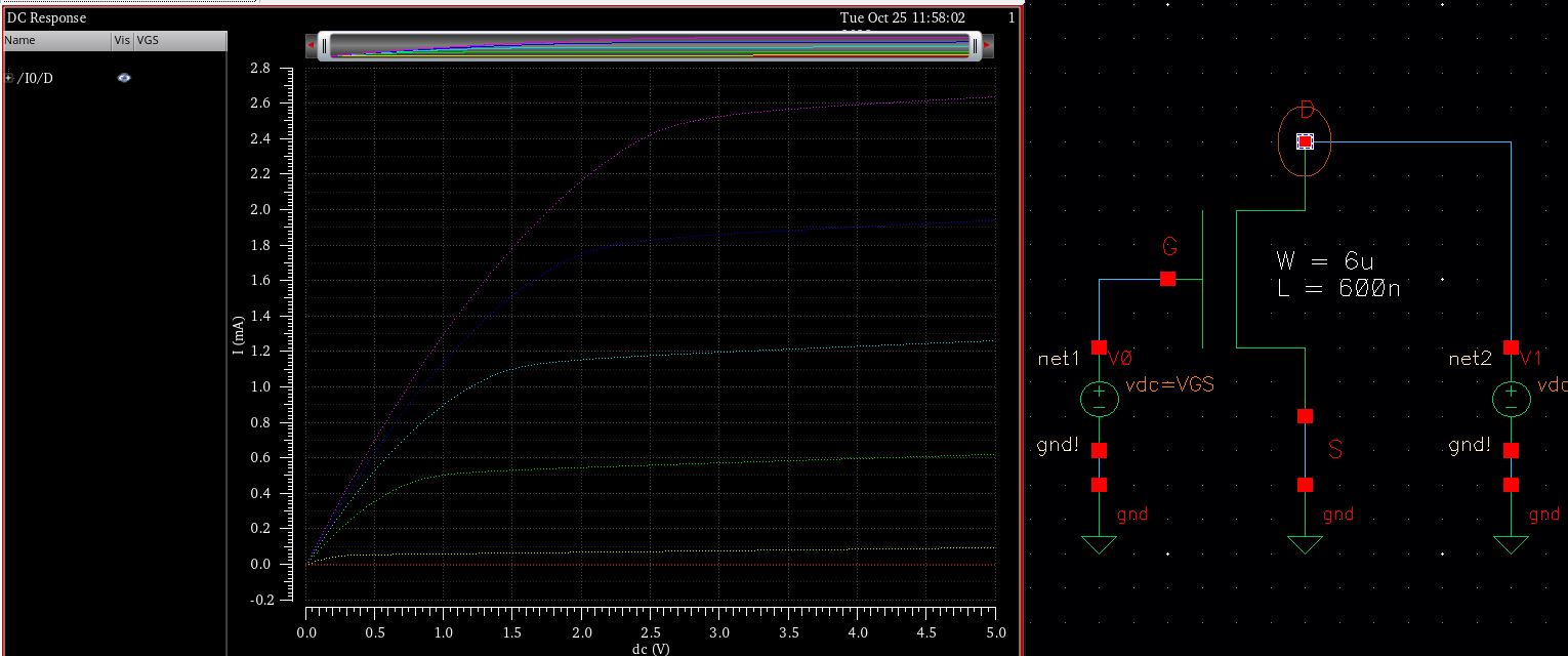
Figure 4: NMOS symbol simulated in Cadence.
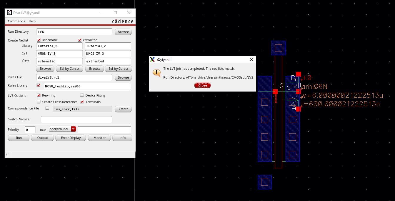
Figure 5: NMOS extracted layout view with completed LVS check.
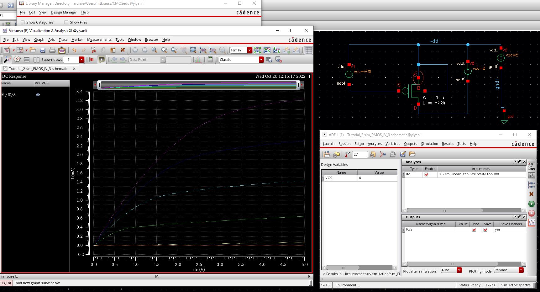
Figure 6: PMOS symbol simulated in Cadence.
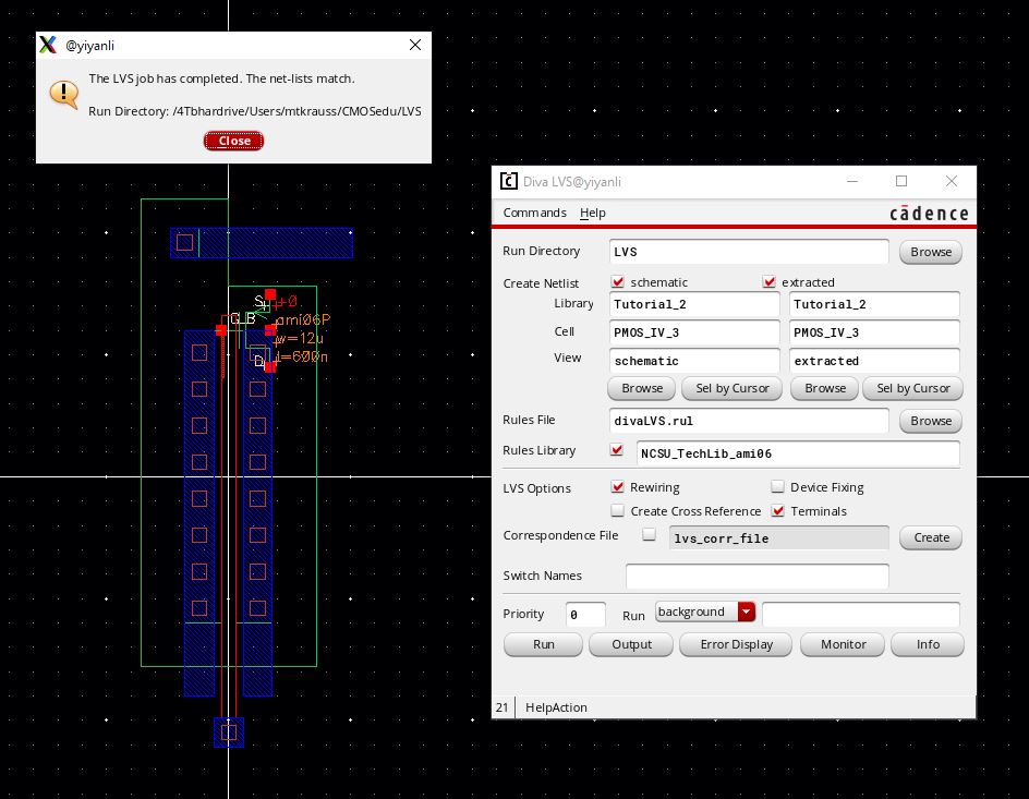
Figure 7: PMOS extracted layout view with completed LVS check.
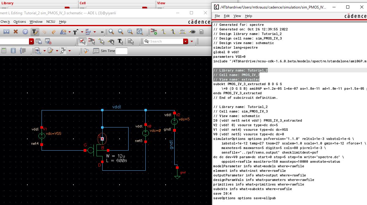
Figure 8: Netlist display showing simulation ran using extracted view. Graph is identical to the one in Figure 6.