CE 433
Comboblocks
Name: Max
Krauss Email:
mtkrauss@fortlewis.edu
Combinational
Logic Blocks
Tasks 1.
Repeat the simulation of Half Adder and Full Adder in Section 1. (10
points)
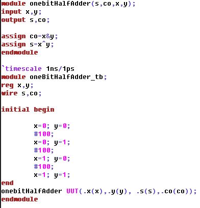
Figure 1: GVIM code for the 1-bit HA.
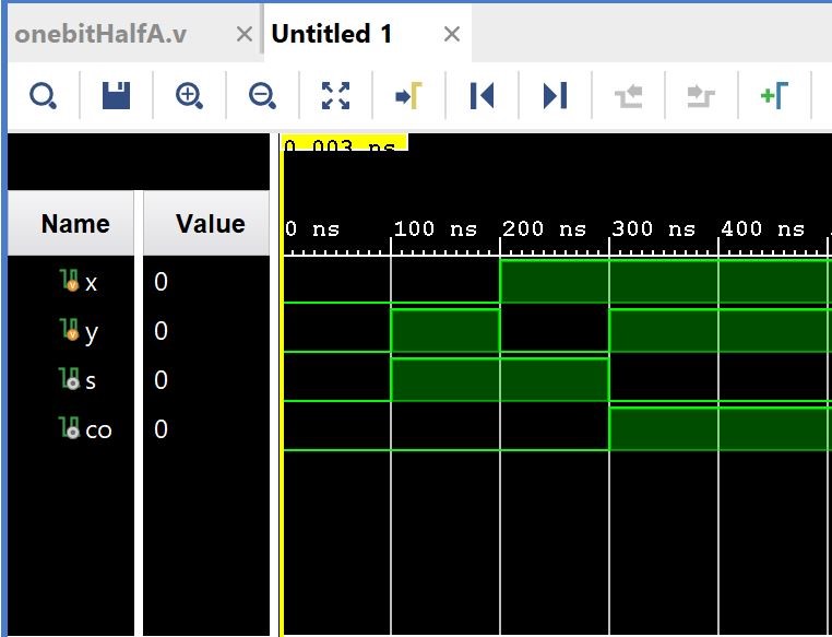
Figure 1.1: Vivado Simulation for the 1-bit HA
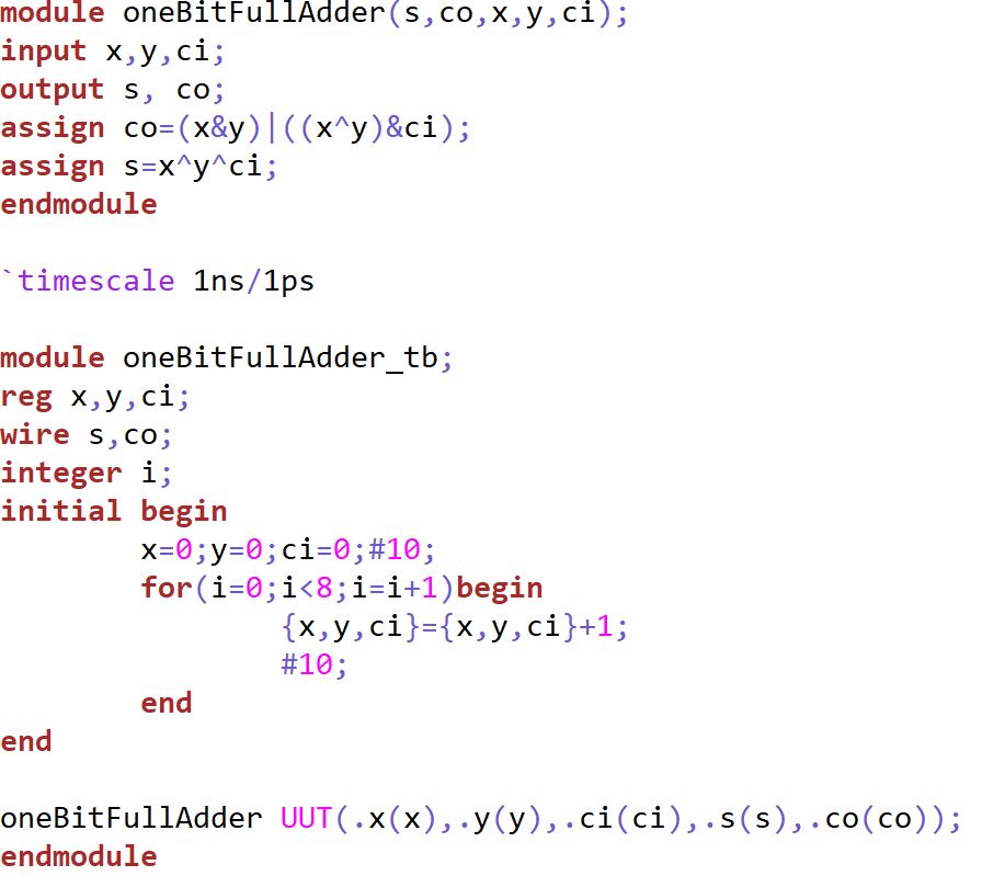
Figure 1.2: GVIM code for the 1-bit FA
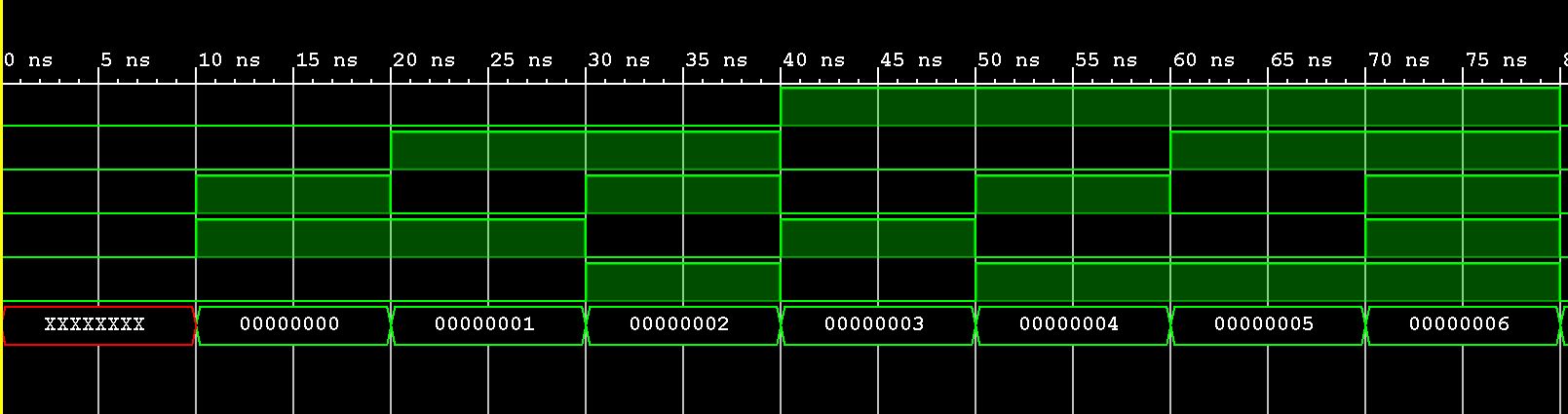
Figure 1.3: Vivado Simulation for the 1-bit FA.
2.
Design the testbench for the comparator in Section 2 and show the
simulation results. (10 points)
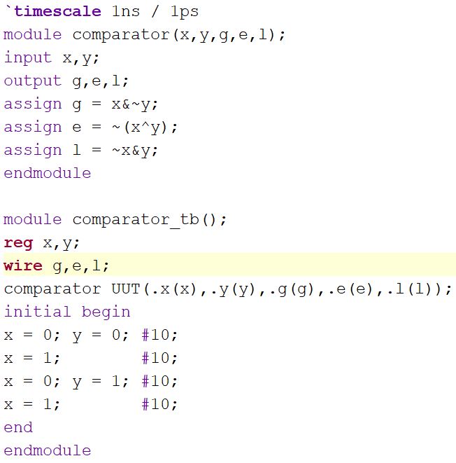
Figure 2: GVIM code for the comparator.
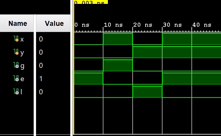
Figure 2.1: Vivado simulation for the comparator.
3.
Design the testbench for the 4-bit comparator in Section 3 and show the
simulation results. (10 points)
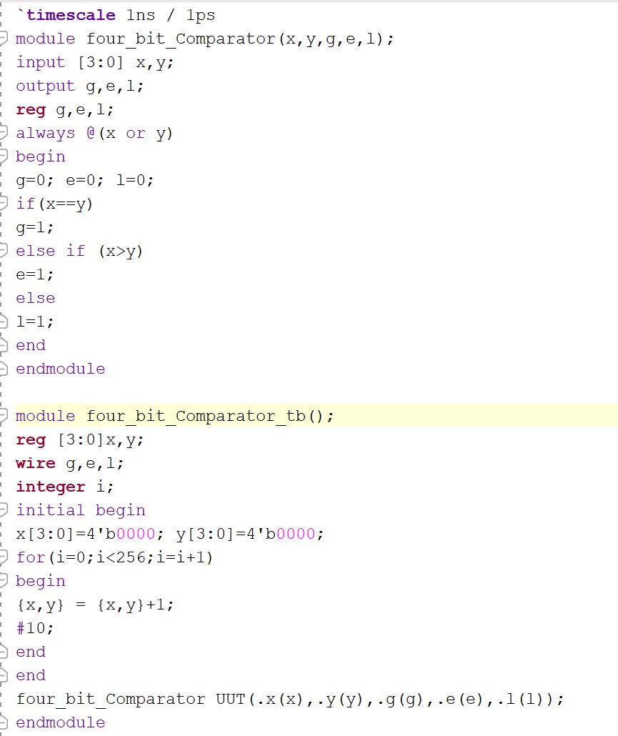
Figure 3: Verilog Code for the 4-bit comparator.
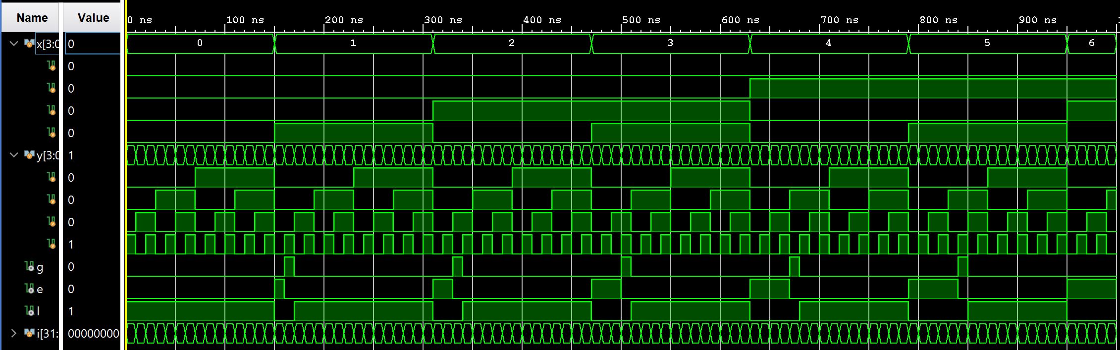
Figure 3.1: Vivado simulation of the 4-bit comparator.
4.
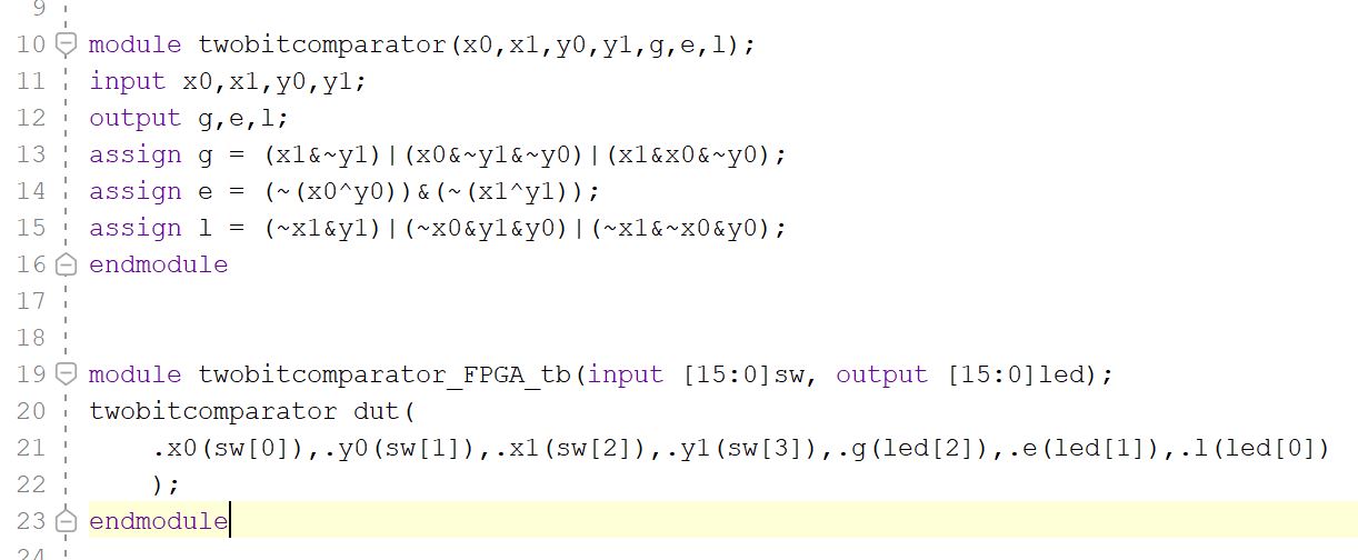
Implement a 2-bit comparator on the Basys 3 board. Use sw as inputs and
led as outputs. (10 points)
Figure 4: Verilog code for the 2-bit comparator.
As you can see, I simply used gate level logic to program the FPGA.
Embedded below is my video demonstration.
5.
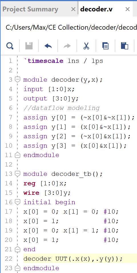
In Section 4, design the testbench for the decoder and verify the logic
in simulation (use the Dataflow modeling method). (10 points)
Figure 5: Verilog Code for the decoder.
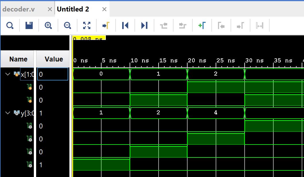
Figure 5.1: Vivado simulation for the decoder.
6.
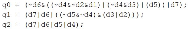
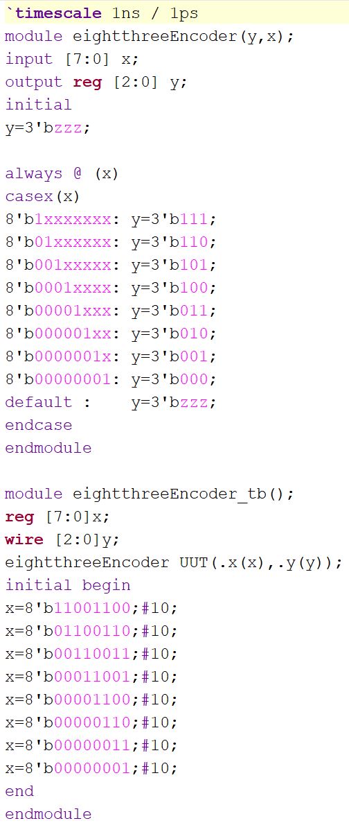
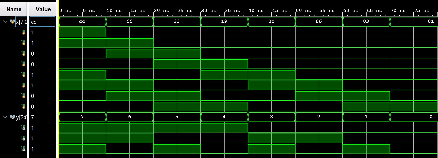
In Section 5, for the 8x3 priority encoder, find Q2 and Q1, build the
module and verify the logic using simulations. (10 points)
Figure 6: Logic for Q0,Q1,and Q2.
Figure 6.1: Verilog code for the 8-3 Priority Encoder.
Figure 6.2: Vivado simulation for the 8-3 Priority Encoder.
7.
In Section 6, implement a 4-1 multiplexer on your Basys 3 board. Show
embedded Youtube video demonstration on your report. (10 points)
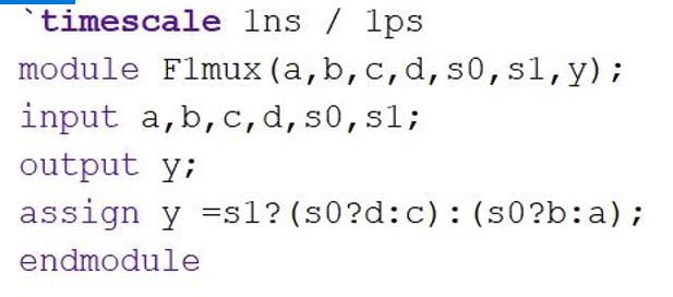
Figure 7: Verilog code for the main 4-1 Multiplexer module.
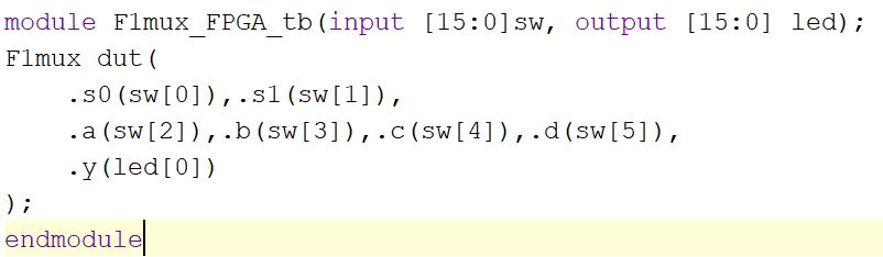
Figure 7.1: Verilog code for the 4-1 Multiplexer FPGA testbench.
Embedded below is my 4-1 Mux verification video.
8.
Design/verify an even parity generator and checker in simulation
respectively. Implement an even parity checker on your Basys 3 board -
use sw as inputs, use leds as output indicators. Show embedded Youtube
video demonstration on your report.(10 points)
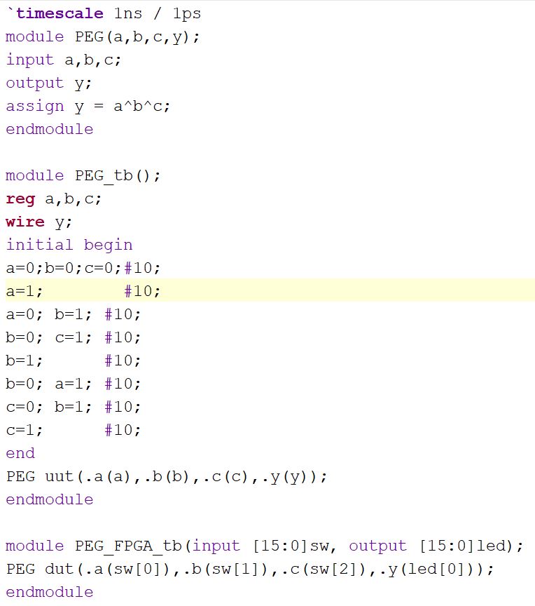
Figure 8: Verilog code for the Even Parity Generator.
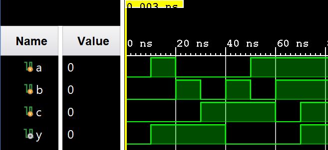
Figure 8.1: Verilog Simulation for the Even Parity Generator.
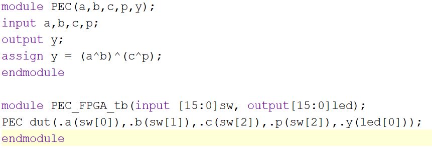
Figure 8.2: Verilog code for the Even Parity Checker.
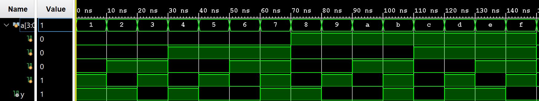
Figure 8.3: Vivado demonstration for the Even Parity Checker.
Embedded below is my EPC verification video.
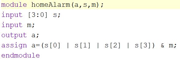
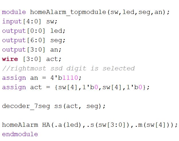
9.
Implement the design in Section 8 and Section 9 on your Basys 3 board.
Show embedded Youtube video demonstration on your report.(20 points) Upgraded home
alarm system
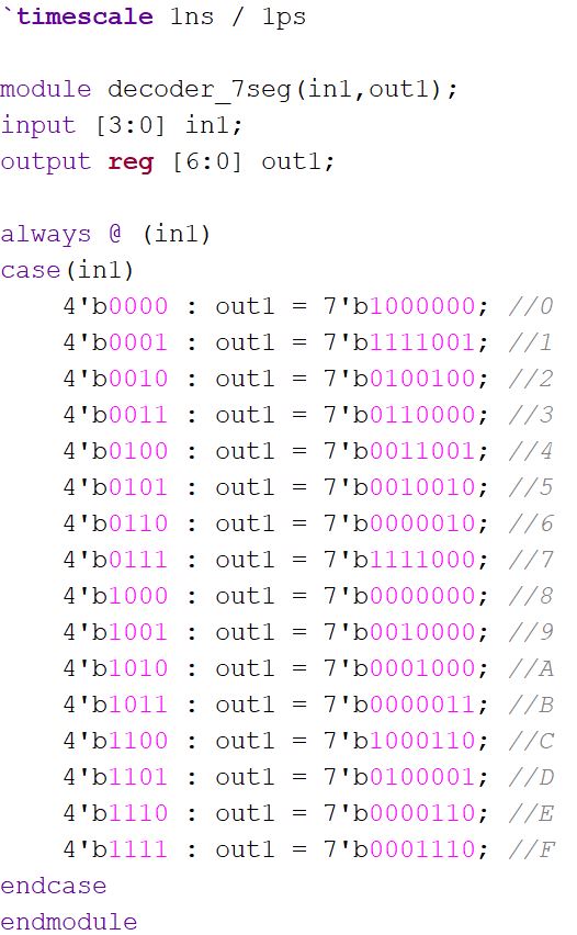
Figure 9: Verilog code for the SSD decoder.
Figure 9.1: Verilog code for the upgraded home alarm module.
Figure 9.2: Verilog code for the top module of the upgraded home alarm
system.
Embedded below is my upgraded home alarm system verification video.
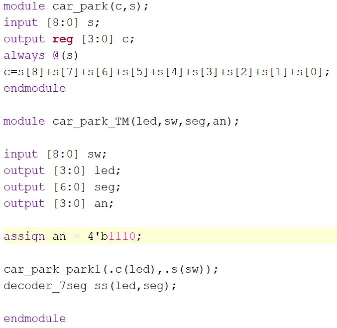
Upgraded parking
counter
The following top module also utilized the SSD decoder module from
figure 9.
Figure 9.3: Verilog code for the main and top module of the upgraded
parking counter.
Embedded below is my upgraded parking counter verification video.
Results: This tutorial demonstrated how there are many different
methods to code combonational logic blocks. Verilog code paired with
Vivado and a Baysys 3 allow one to literally code logic and then verify
it with their hands. A fun way to learn combonational logic and apply
it in the real world.