ENGR338 Lab 2022
Fall
Lab 4 MOSFETs
and IV Curves
Name: Mason
Brady
Email:
mrbrady1@fortlewis.edu
MOSFETs
and IV Curves
Introduction:
This lab uses Electric VLSI and LTSpice to simulate pmos and nmos gates.
Materials:
LTSpice, Electric VLSI
Methods:
First, an NMOS was placed and the spice-model was set to NMOS as per
the simulation file. This was repeated for the PMOS as well before
layouts of each were made.
The layout was made using and nMos node and two nAct nodes which
functioned as the drain/sink for the node. A metal1 to poly pin was
placed allowing a metal 1 arc to be used to connect to the gate. For
the NMOS node, a pWell was used to ground the gate to the body of the
chip. The width of every component(except the metal1-poly pin) was set
to 10 before the nodes were connected as seen below.
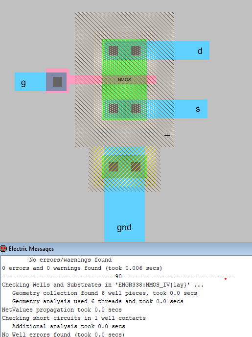
Figure 1.
NMOS layout completed with 0 errors.
The same process was completed for the PMOS circuit using an nWell for
ground and pAct/pMos accordingly. This can be seen below in Figure 2.
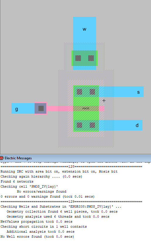
Figure 2. NMOS
layout completed with 0 errors.
Both of these layouts passed both DRC and NCC checks as seen in the
screenshots and were simulated in LTSpice which can be seen in the
Results section(Figure 4 and 5).
The schematics were then completed similar to the layouts
so that they had connections and the whole thing passed NCC. The
connections were straight forward and can be seen below in Figure 3 and
Figure 4.
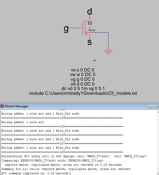
Figure 3. Nmos
schematic connections and NCC results.
This was fairly straightforward and simulation code was written to
simulate the file. These results were the same as the original
simulation and can be seen below.
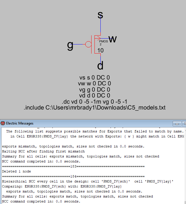
Figure 3. Pmos
schematic connections and NCC results.
Results:
Both circuits were simulated and got the following results.
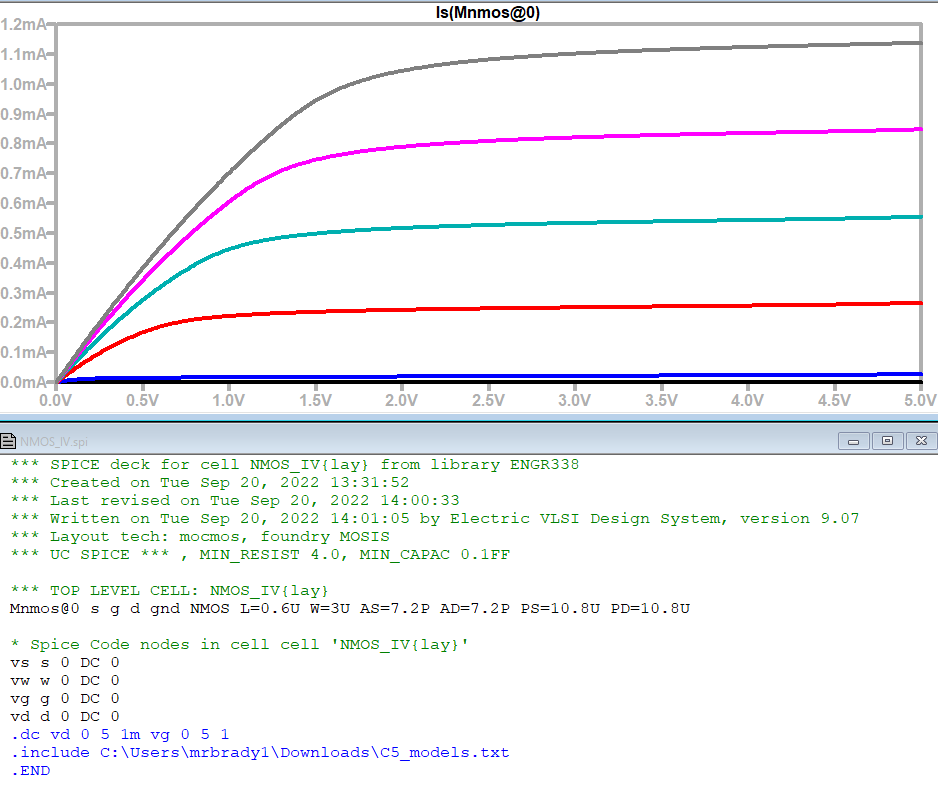
Figure 4. Simulation
results for NMOS transistor as Vd and Vg were changed from 0 to 5V
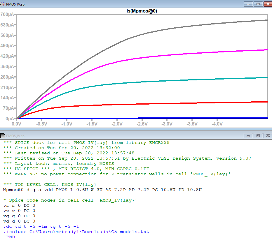
Figure 4. Simulation
results for PMOS transistor as Vd and Vg were changed from 0 to 5V
Discussion: The simulation results
were a
little weird. I flipped the voltages to negative for some reason in my
PMOS circuit which
resulted in me getting nearly identical graphs between the two. I'm not
sure what my logic behind this was but the true graphs should be mirror
images of each other.