Embedded Systems
Spring 2024
HW 3 Combinational
Logic Blocks Name: Mason
Brady Email:
mrbrady1@fortlewis.edu
HW 3
Introduction:
This homework is an introduction to Combinational Logic Blocks
Materials:
gvim, vivado, basys 3
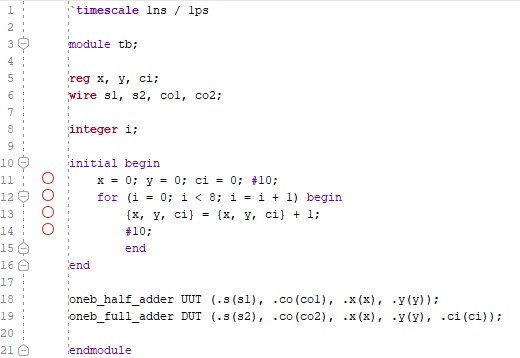
1) 1/2 and Full Adder The
full and half adder modules were written as seen below in Figure 1.
Another way of doing this would be to feed the output of the half adder
into a second half adder but the logic for the full adder is pretty
straight forward so it was simpler to just write a new module. Figure 1. Full
and Half Adder Modules.
The test bench was then written so that I could test both adders
simultaneously for reasons mentioned in past assignments. Figure 2. Full
and Half Adder Test Bench.
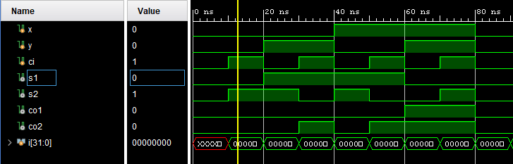
Because I combined both modules into the same simulation the graph is
slightly harder to read but the output for the half adder is S1 and Co1
while the full adder is connected to S2 and Co2. Figure 3. Full
adder and half adder simulation, the output for the FA is S2
and Co2 while the half adder is S1 Co1.
2) 2-bit Comparator
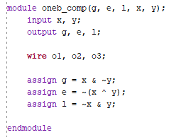
The two bit comparator was pretty straight forward, the
module can be seen below. I'm not entirely sure what I was doing with
the o1-3 wire and it can be ignored. Figure 4. One
bit comparator module.
The test bench was nearly identical to the adders just changing the
number of iterations needed to check the logic and obviously there is
no carry. Figure 5. One
bit comparator Module. The
simulation is exactly what one would think, if x > y then g is
on, x < y l is on, and if they are equal is is pulled high. Figure 6. Two
Bit Comparator Simulation.
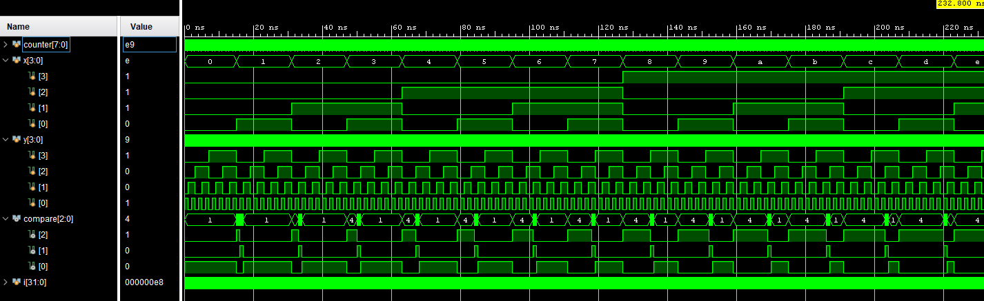
3) 4-bit Comparator
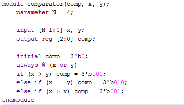
The
logic for the four bit comparator was again very straight forward, I
changed the output to be a 3 bit register so it was easier to read than
3 individual bits if I use this in the future. Figure 7. N-Bit
Comparator Module.
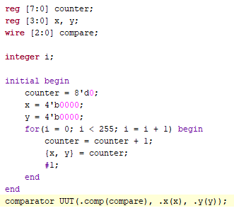
The test bench for this module I had some issues with. My
for loop was refusing to work for some reason. I rewrote the exact same
loop in the same test bench file for the MUX later on and it worked for
the MUX so I just pasted my testing logic for the comparator in and it
magically fixed itself. I thought it was an issue with the simulation
settings but that ended up not being the case. The only thing I changed
when it worked was reducing the delay from 10ns to 1ns but I doubt that
changed anything since it wasn't an issue of the code running too long
(I initially had it with a 10ns delay and the logic worked properly for
the MUX it just ran out of simulation time before reaching the full 256
iterations). Figure 8. N-bit
comaprator test bench.
The
simulation shows the inputs x and y incrementing and the comparisson of
the two. Compare[0] is x < y, Compare[1] is x = y and Compare
[2] is x > y which becomes more frequent after the first half of
the simulation since it takes a while for x to start incrementing with
how I setup my TB. Figure 9. N-bit
comparator (4bit) Simulation.
4) 2-bit Comparator on Basys Board For
this section I took the N-bit comparator and reduced N to 2 and then
wrote the test bench seen in Figure 10. Figure 10.
2-bit comparator for Basys 3 Upload.
The video of this working on Basys 3 board can be seen below. The
first two switches are X and the second two switches are Y. The first
LED is X < Y, Second LED is equals, and the third is X > Y.
Figure 11. Basys 3 Board Demo of 2-bit Comparator.
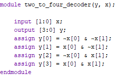
5) Decoder
Two bit to four bit decoder was written and can be seen below in Figure 12. The logic is very simple. Figure 12. 2-4 Bit Decoder.
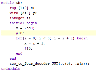
The test bench is nearly identical to all the other test benches in this writeup. Figure 13. Test bench.
The logic was simulated and can be seen below. Figure 14. Decoder Simulation, Y is output X is input.
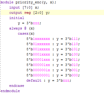
6) 8x3 Priority Encoder The
priority encoder was written using the casex which allows for general
cases where not every bit is known but doesn't need to be known. Figure 15. Priority Encoder Module.
Again, another nearly identical test bench. Note the 1ns delay or else it gets really long. Figure 16. Priority Encoder Test Bench.
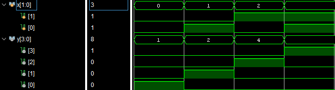
Priority encoder was then simulated and can be seen below. One note
is that at x = 7'd0 the encoder output is a NAN value since that is the
default case. Figure 17. Priority Encoder Simulation.
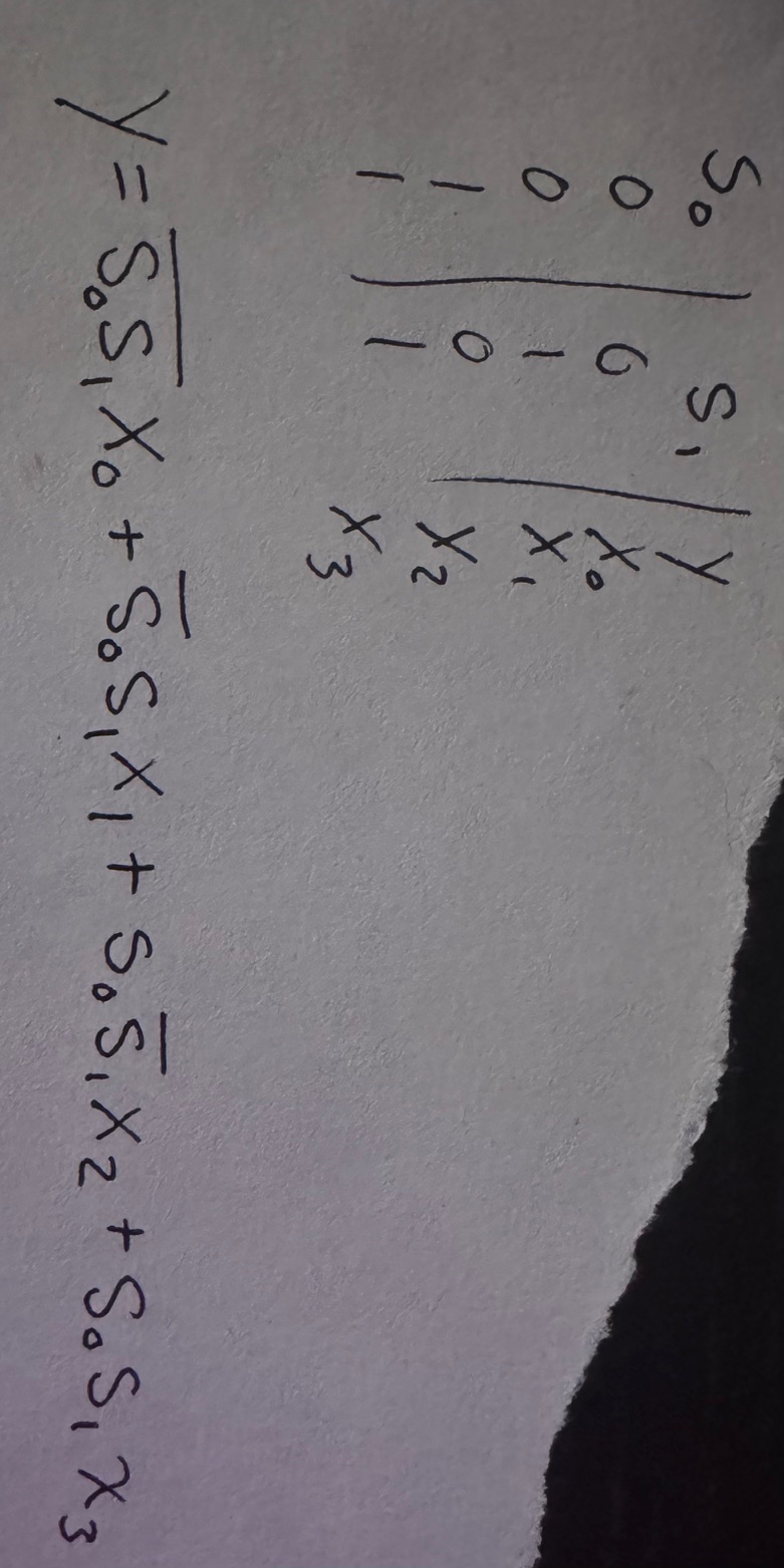
7) 4-1 Multiplexed Logic
Derivation I think
I did what was being asked for this part? The question was kind of
vague and what I did was very straight forward so it seems like I did
something wrong but I'm not really sure what else we are supposed to
do. The gist is that S0 and S1 control which input we pass to the
output. \ Figure 18. MUX Logic "Derivation".
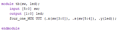
8) 4-1 Multiplexer on Basys Board The same 4-1 MUX Module as in the lab was used. The test bench for the Basys 3 can be seen below in Figure 19. Figure 19. Basys 3 Test Bench for 4:1 MUX.
The
demo on the board can be seen below in Figure 20. The first four
switches are the inputs and the 5 and 6 switch is the selection bits.
The first LED displays the output.
Figure 20. Basys 3 4:1 MUX Demo.
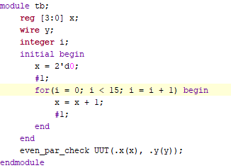
9) Even Parity Generator and
Checker - Chcker on Basys Board
Even parity generator and checker logic is pretty simple and
I wrote both modules at the same time and then simulated them
seperatly. Theoretically you could somewhat test them by running both
simultaneously by feeding the generator output into the input of the
checker and making sure it always 0. Another thing I did slightly
diffrently from the tutorial is output y as the whole output not just
the parity bit. Again, I did this to future proof the module incase it
comes up in another assingment so I don't have to concatenate the
output later on. Figure 21. Even parity generator and checker modules.
The
test benches were fairly similar I just had to flip the size of x and y
to the correct sizes. I'm now realizing I forgot to take a screen cap
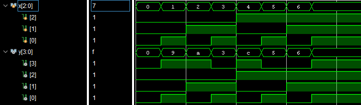
of the TB for the generator but I have the simulation below. Figure 22. Even parity check test bench.
I ran both simulations and they went pretty straight forward. Figure 22. Generator Simulation. Figure 23. Checker Simulation.
I then uploaded the checker to the Basys 3 and also forgot to take
a screen grab of the TB before writing over it with the next part. All
I did was switch the input from a generated input to be switches 0-3
and the output was just LED 0 as seen in the video
Figure 24. Checker Demonstration on Basys 3.
10) Improved home alarm and car
parking spot counter
For
this section I coppied my home alarm and car parking spot modules from
the last assignment and tacked on the rest. The first step was writing
the 7-Segment display conversion which seems like it will be a useful
module going forwards. Basically the module is just a big case which
allows easy conversion from 0-9 and A-F to g-a bit designations that
can be input to the ssd. The home alarm code was otherwise unchanged
and the parking count logic was simplified into a basic sum. Figure 25. Home Alarm, Car Count, and SSD Modules.
The test bench for the home alarm was pretty simple just had to
define which ssd to use and setup the switches and LED for displaying
when the alarm has been "tripped" and activated. Figure 26. Test Bench for Home Alarm with Seven Segment Activation Display.
The Basys 3 Demo can be seen below
Figure 27. Basys 3 Demo of Home Alarm 2.0.
The test bench for the parking count was very similar and can be seen below in Figure 28. Figure 28. TB for Parking Count 2.0.
And was demoed on the Basys 3.
Figure 29. Basys 3 Demo of the Parking Counter.
Discussion: This
weeks work felt very long and some of the tasks felt repetitive and
redundant (Doing MUX several times and the large version of simple
gates). Other than that the code was striaght forward, just seemed like
it didn't stop. I also got very lazy with the writeups towards the end.


 \
\