ENGR338 Lab 2022
Fall
CADENCE TUTORIALS
Name: Mason
Brady
Email:
mrbrady1@fortlewis.edu
Cadence Tutorials 1 and 2
Introduction:
This lab uses cadence tools and software to build and layout simple
gates.
Materials:
Cadence
Methods:
First cadence was setup by following the initial tutorial, I didn't
take any photos of this because it didn't feel like much of an
accomplishment, more of a stepping stone to the real lab.
The first step was creating a simple voltage divider circuit using 10k
ohm resistors. This can be seen below in Figure 1.
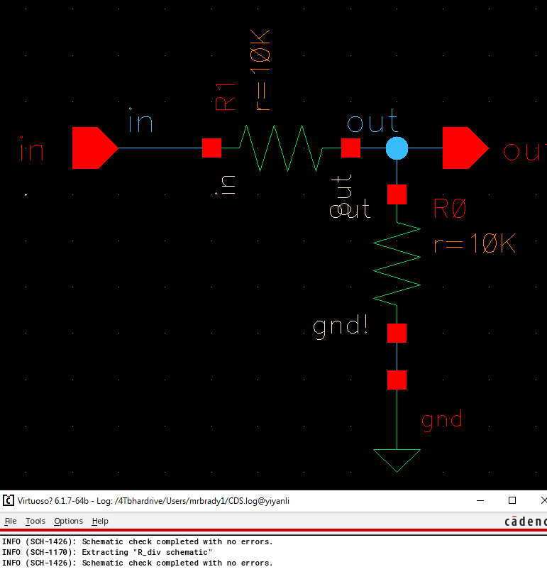
Figure 1.
Voltage Divider Schematic.
Pins were then added to the schematic on the in and out pins as seen
below in Figure 2.
Figure 2. Schematic
with import/export pins
A
symbol view was then created for the design and added into another
schematic which included a new dc voltage source and a few auxillary
wires.
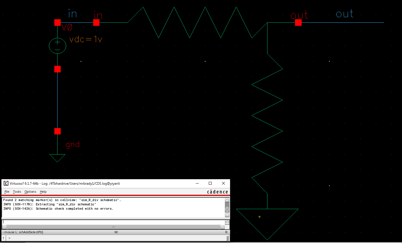
Figure 3. Schematic
using voltage divider icon.
The voltage divider layout was then created by first placing an n-well
and stretching it to 56um by 4.5um. Then two ntaps were added to the
ends of the resistor so that arcs could be connected and res_id was
dragged to cover the resistor. This resistor was duplicated and used
arcs to connect the two terminals creating the vout network and arcs on
the left terminals creating the vdd and ground connections. The layout
can be seen below in Figure 4.
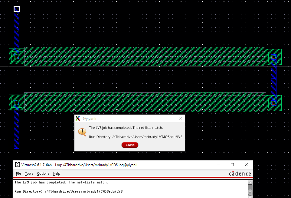
Figure 4. Voltage
divider layout with LVS check.
Now for the real deal. An NMOS was placed in the schematic area with
in/out pins connecting to the GDS. The width was set to 6um and the
length to 600n. The schematic can be seen below in Figure 5.
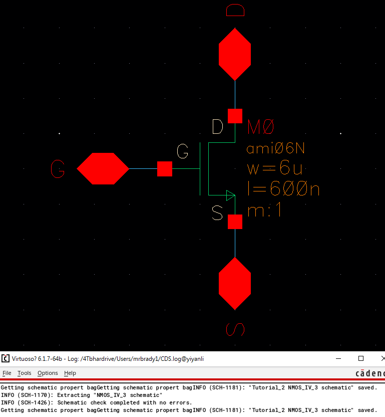
Figure 5. Nmos with
pins schematic.
A new icon was then created for the new 6u/600n NMOS as seen below in
Figure 6.
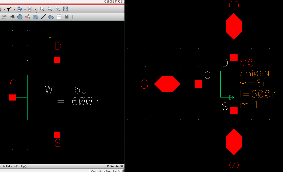
Figure 6. Icon
view(left) of 6um by 600n NMOS gate(right).
Then everybody's favourite part, the layout was created. This was
fairly straight forward except I was having trouble connecting my arcs
to the NMOS drain and sink, they kept not wanting to make an actual
connection and then had overlap errors. After deleting and replacing
the arc several times however it seemed to eventually work. A ptap and
a poly-metal1 via was placed. The gate was wired to the via and the
sink/drain were wired to pins labeled accordingly. The via was also
given a pain appropriately labeled G. The ptap was labeled ground.
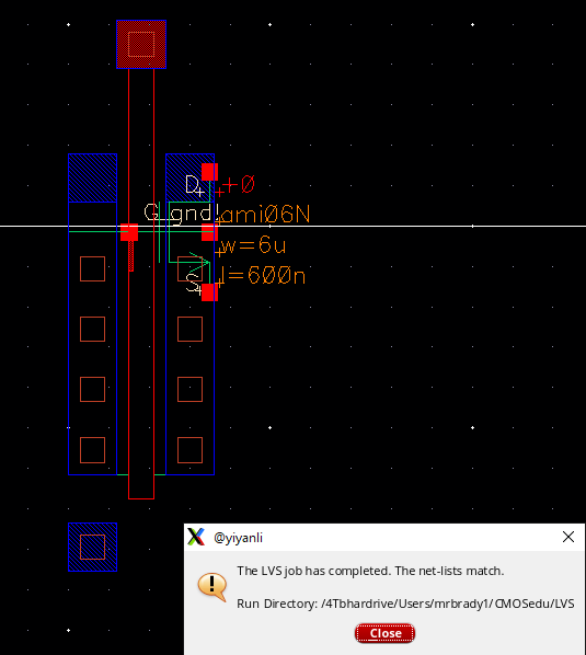
Figure 7. NMOS
gate passing LVS.
The same process was repeated for PMOS and can be seen below. The Icon
and Schematic were created for the PMOS in an identical way using the
existing PMOS gate with a width of 12u and 600n for length. 2-way pins
were shorted to each terminal and labeled accordingly. The result can
be seen below in Figure 8.
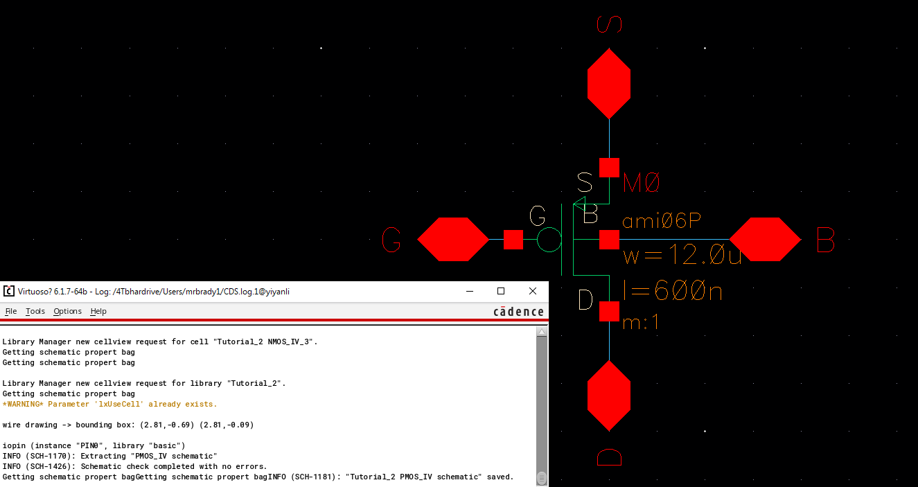
Figure 8.
PMOS Schematic.
The icon was also almost identical except with a small circle ontop. It
can be seen below in Figure 9.
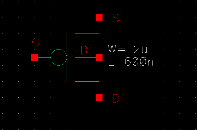
Figure 9. PMOS
icon.
Finally, it was laid out using an ntap instead of ptap and everything
else being the same.
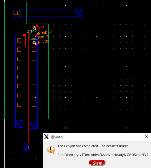
Figure 10. PMOS
layout.
Results:
The voltage divider, NMOS, and PMOS were all simulated and the results
were as expected. For each simulation the extracted layout view was
also simulated and yielded identical results so I didn't take an extra
screenshot.
The voltage divider was simulated using a spectre simulation and a
constant vdd of 1V. The simulation can be seen below in Figure 11.
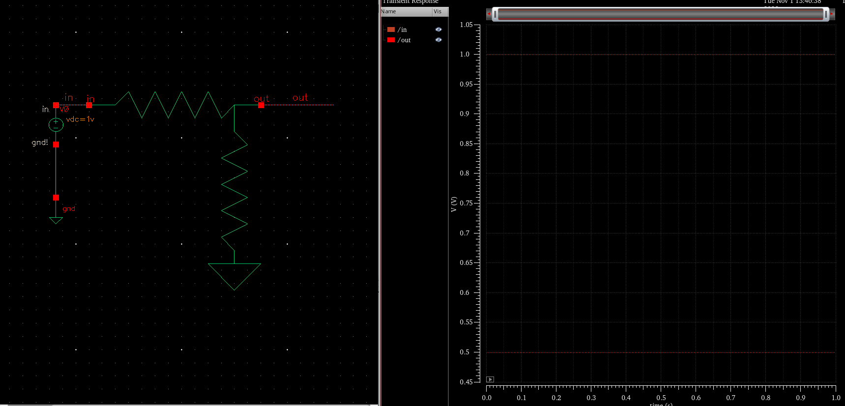
Figure 11. Voltage
divider simulation input 1V and 0.5V output.
A parametric linear sweep Spectre analysis was used for the PMOS and
NMOS to create IV curves with varrying gate voltages. The NMOS curves
can be seen below in Figure 12. where the gate voltage ranged from 0 to
5V.
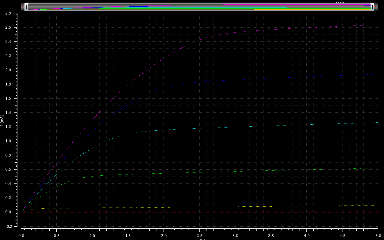
Figure 12. NMOS
simulation
The same process was used to simulate the PMOS.
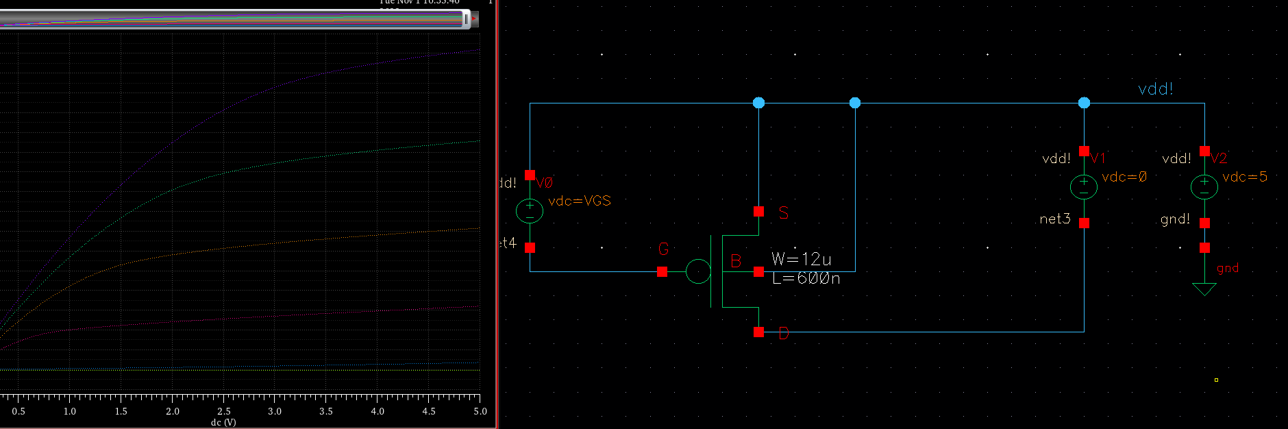
Figure 13. PMOS
simulation results
Discussion: It was
cool to use the industry standard software but it was tricky to learn
all the nuances especially when it came to creating simulations.