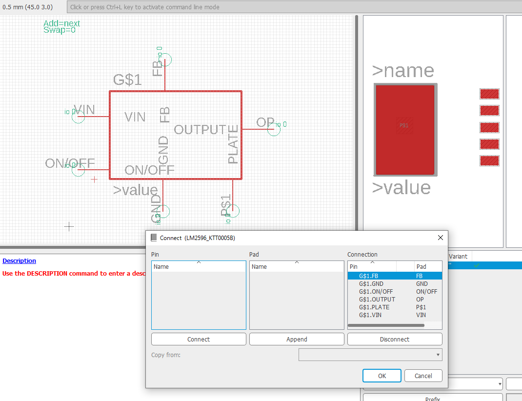
Next a symbol for the LM2596 voltage regulator was designed and stored in the self created library in Eagle. This is one of a few devices that was created in my personal library or modified using the sparkfun libraries in Eagle.
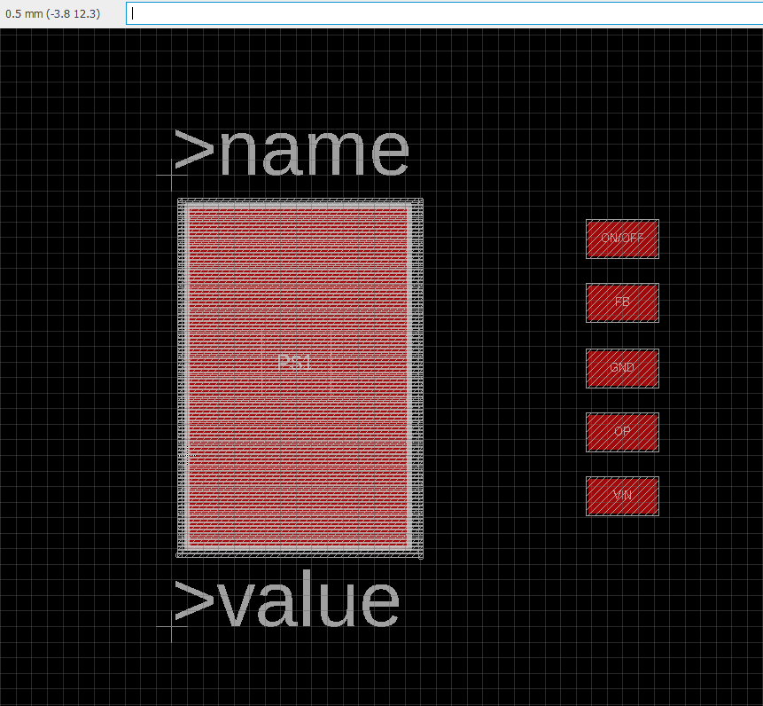
An image of the accompanying footprint for the LM2596 voltage regulator.
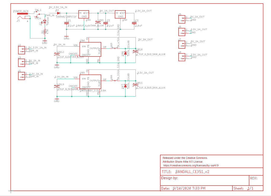
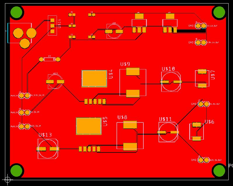
All parts were added to a new schematic and assembled, as shown, in the final schematic below.
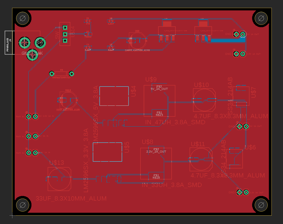
5mm (diameter) mounting holes were added and wires autorouted. Once job was completed a copper pour was added, by way of ratsnest, to the top (red) and bottom (blue) of the board.
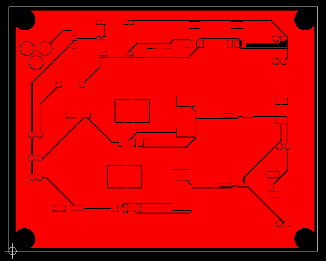
The drill files were compiled with the gerber files and submitted to an online viewer where a final inspection was completed. Below is the resulting image of the coppertop only.
An image of the coppertop and soldermask.
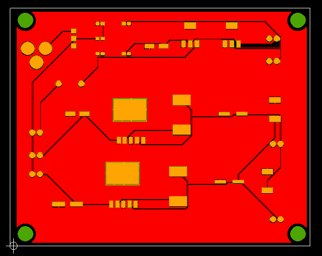
An image of the coppertop, soldermask, and silkscreen.
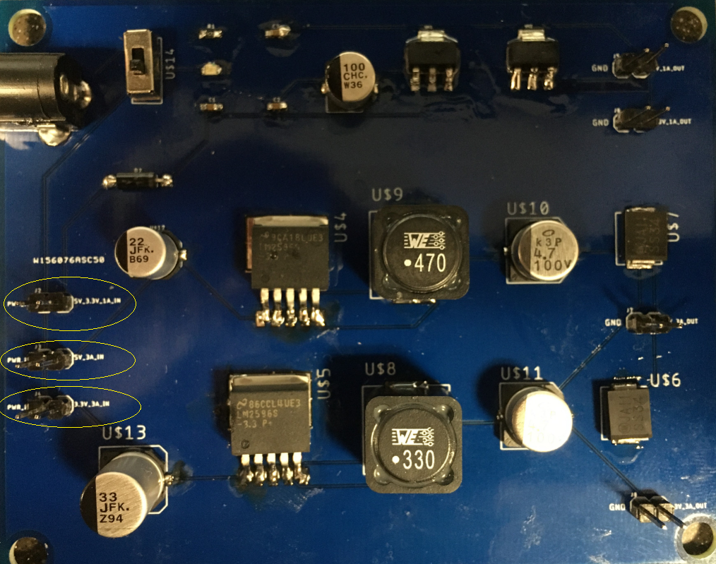
Soldering and PCB Test
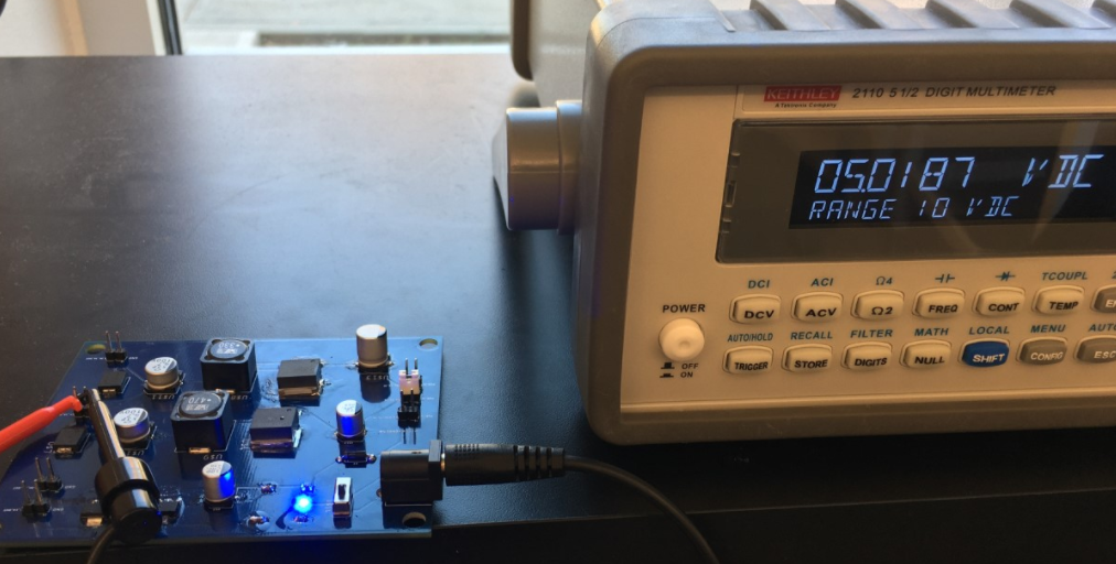
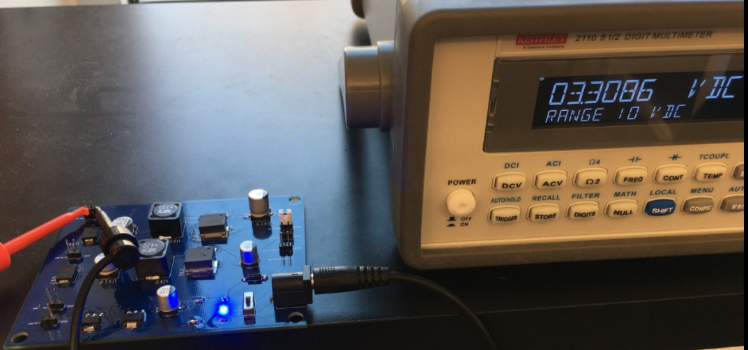
Each component was soldered to the board. A final test was conducted using the highlighted pins to check for functionality.
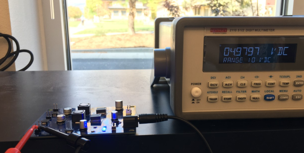
PCB test output voltage at 5V, 1A.
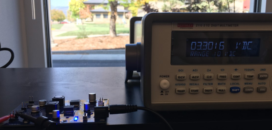
PCB test output voltage at 3.3V, 1 A.
PCB test output voltage at 5V, 3A.
PCB test output voltage at 3.3V, 3A.
Conclusion
The gerber files to the final design of the PCB were submitted for fabrication to PCBway.com and a week later a physical PCB was received. Each component identified in the PCB design was soldered onto the board using solder paste and a soldering rod. Once all components were attached a test of the output voltage was conducted for the 5V_3.3V_1A_IN pin, 5V_3A_IN pin, and the 3.3V_3A_IN pin (highlighted in the photo above). Final results indicate a functioning PCB since testing each pin produced the expected output voltage reading. Recommended design alterations include reducing the physical size of the board to both reduce cost and space occupancy.