CE433 2022 Spring
Week 6
John Hitti
jdhitti@fortlewis.edu
Week 6
Introduction
In this week's
project we will be exploring the basics of the video graphics array
(VGA) display standard by coding programs in Verilog to have our FPGA
output images to a display.
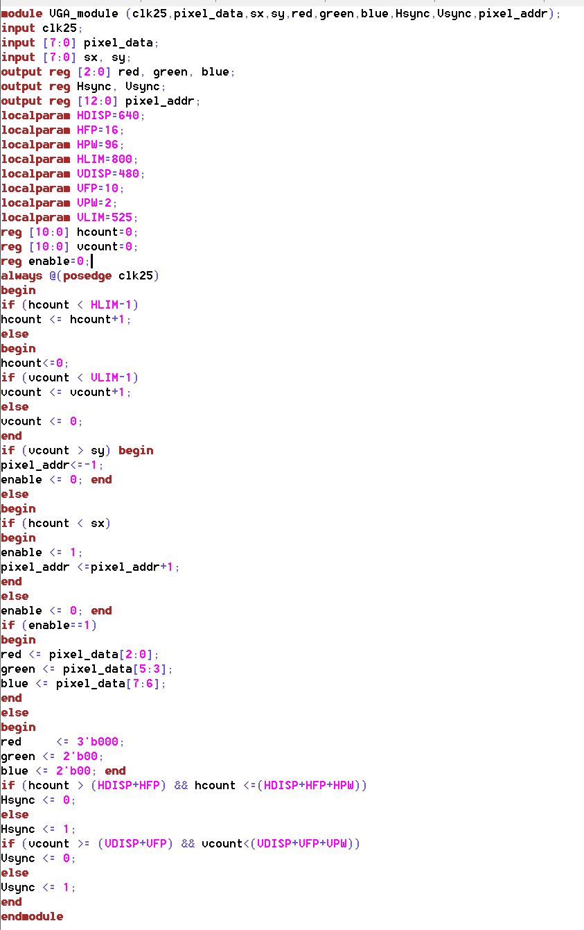
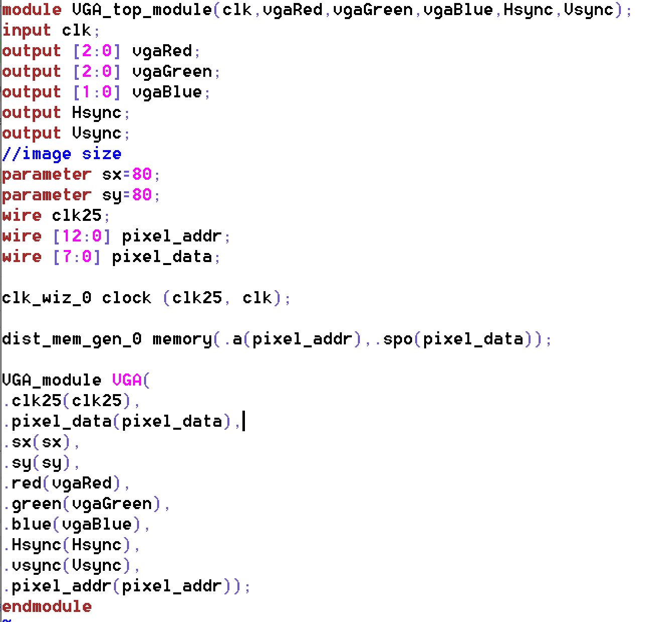
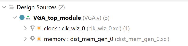
Task 1
In
this task we will use the VGA display port on the FPGA to display a
simple image to a screen. The image data will be stored in a ROM module
and the FPGA will send this data to the display. First we will program
the example code and initialize the clock generator module and ROM
module.
Once this is complete we can upload the program to our FPGA and connect
a screen to verify the functionality.
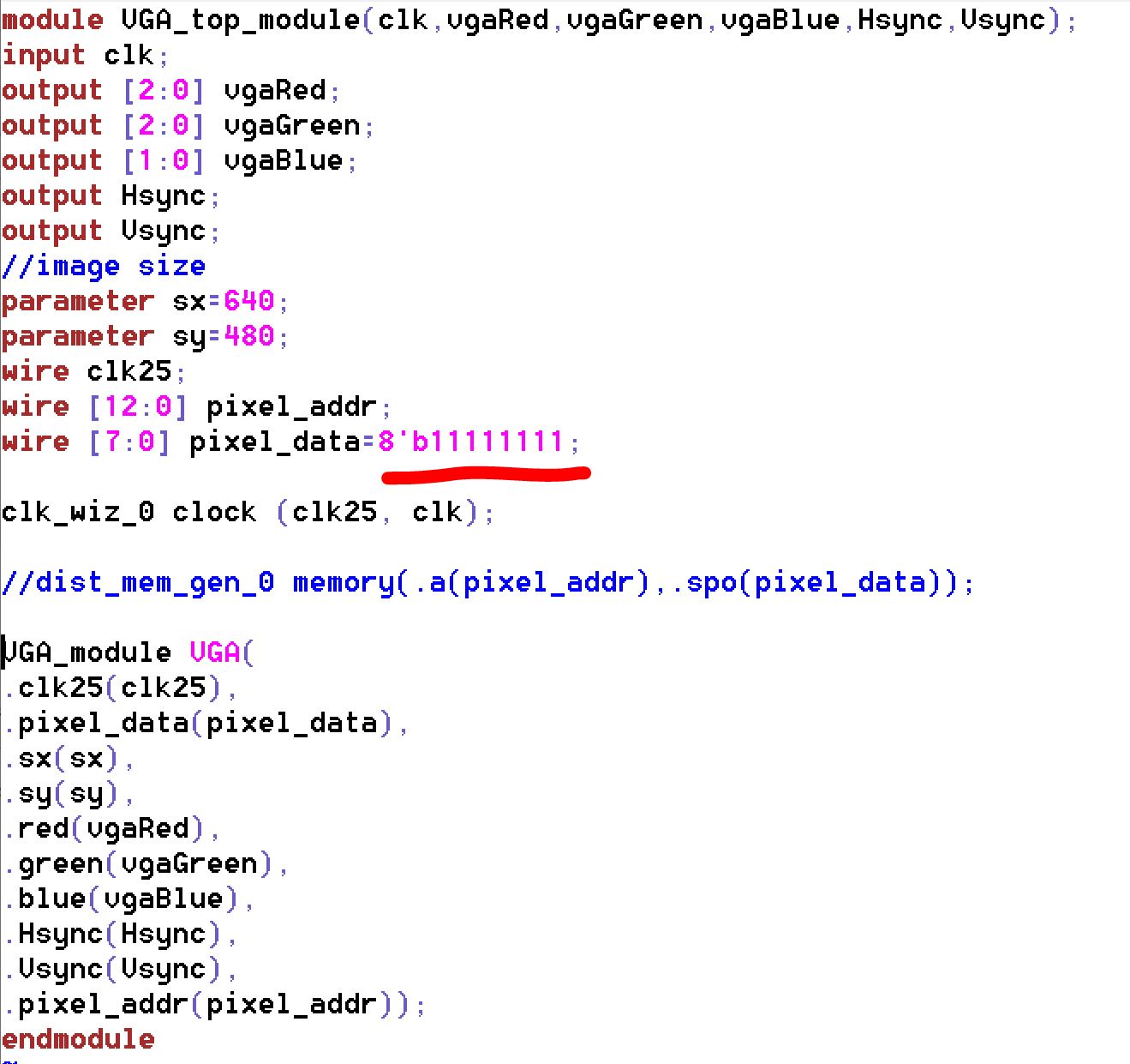
Task 2
In
this task we will be using the same program as the previous task but
modifying it so that the screen will display a white image. First
we modify the program and then we upload it to our FPGA for
verification. We can do this with a very simple modification that is
disabling the ROM in the program and assigning the pixel data to
always be white.
Task 3
In
this task we will take our previous progress further by changing the
display to cycle through a red, green, and blue screen every second. First
we modify the program and then we upload it to our FPGA for
verification. We can do this similarly to the previous task but in
order to cycles through all three colors we need to make a counter that
takes in the clock signal and changes the pixel data based on how much
time has passed.
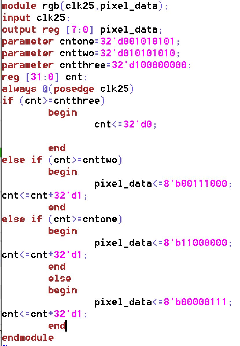
This module is displayed below.
This can then be uploaded to the FPGA. The program appears to be functional! However there is a slight issue with the timing.
Discussion This
project was an excellent introduction to the VGA display standard and
how the FPGA and Verilog can interface with different components such
as displays.