CE433 2022 Spring
Week 3
John Hitti
jdhitti@fortlewis.edu
Week 3
Introduction In this week's
project we will be working with combinational logic blocks in Verilog.
This will include designing, testing, running simulations, and
uploading programs featuring these blocks to out FPGA.
Task 1
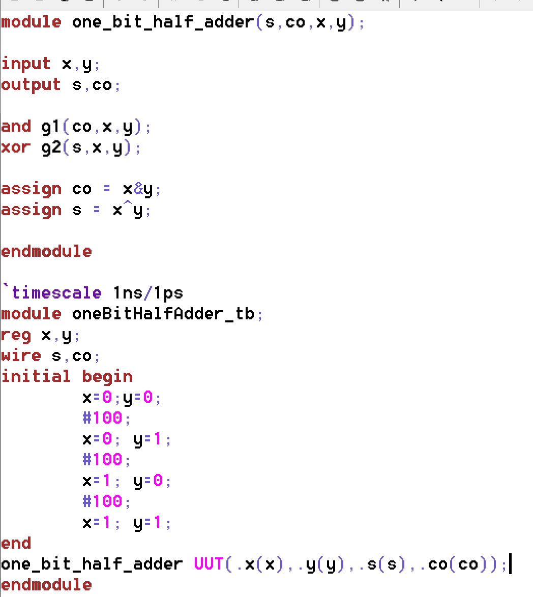
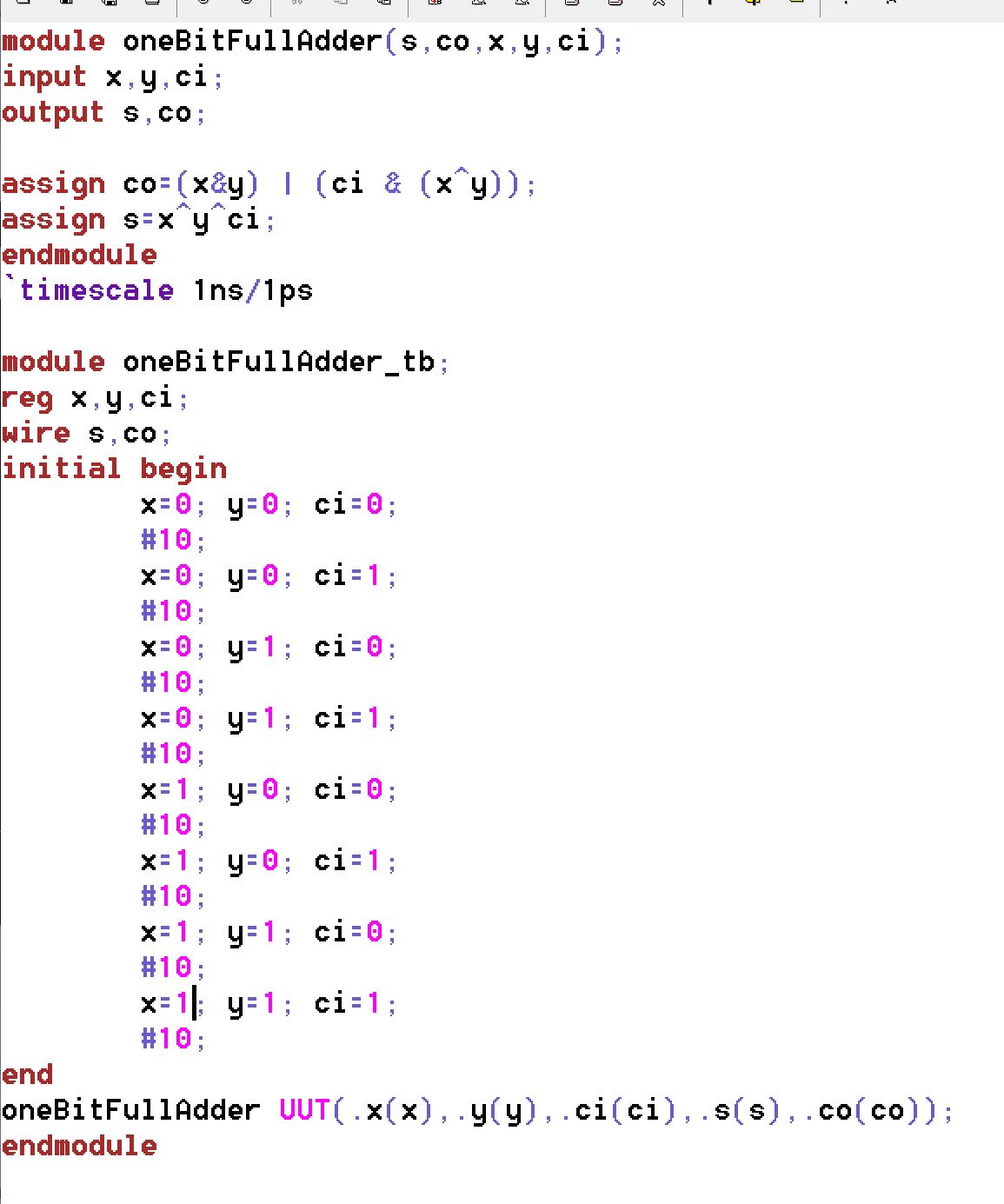
In this task we will be creating a One-bit Half Adder and a One-bit
full adder in Verilog and then running a simulation to verify the
functionality of these adders in Vivado.
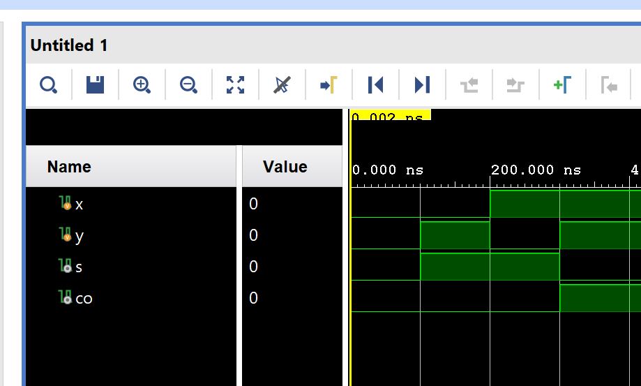
We start with creating the half adder in Verilog with a supporting test bench.
This can then then be run in Vivado to verify the functionality.
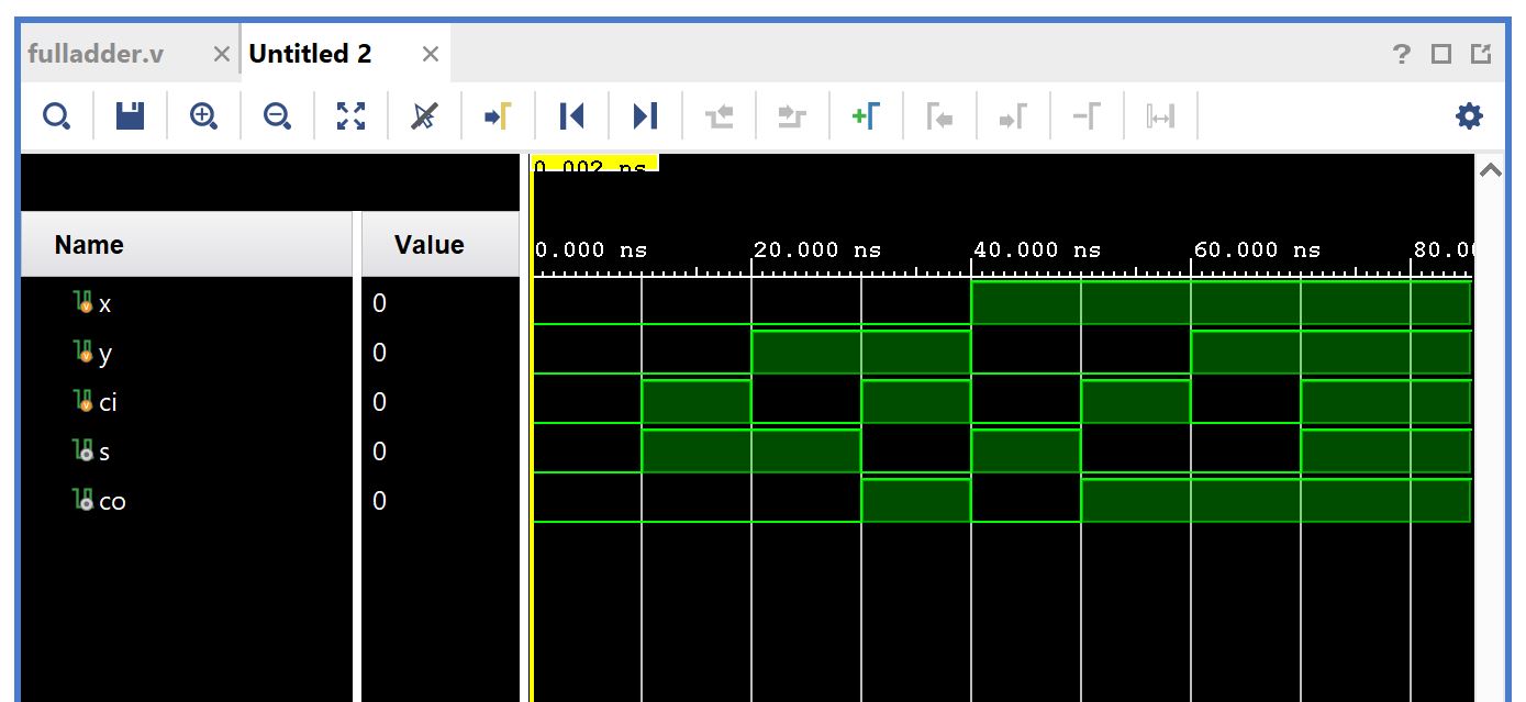
We will then create the full adder in Verilog with a supporting test bench.
This can then then be run in Vivado to verify the functionality.
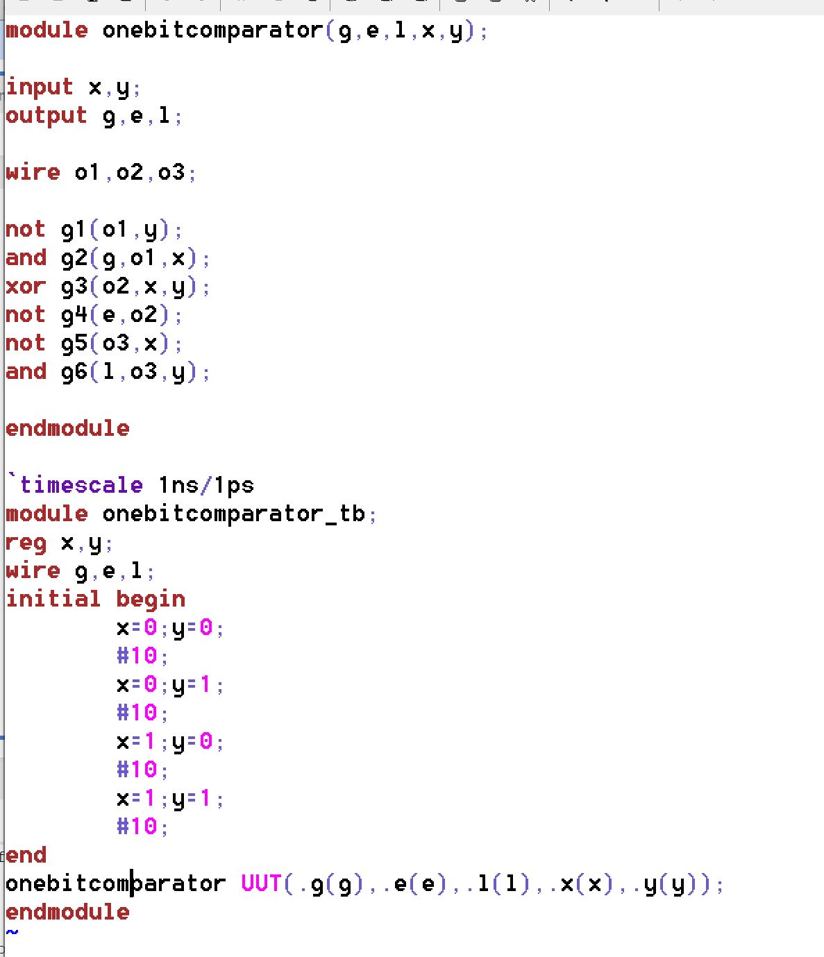
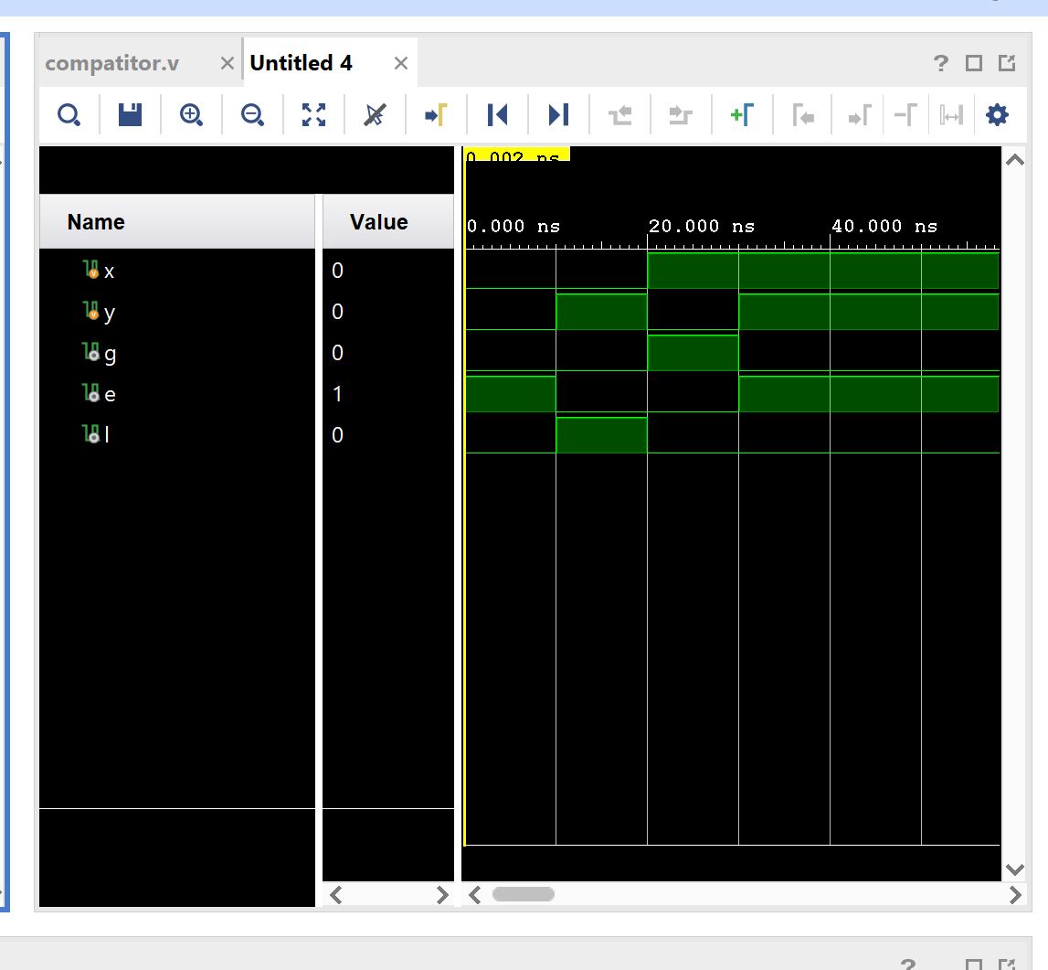
Task 2 In
this task we are to design the test bench for a one-bit comarator
example and run a simulation in Vivado to verify the functionality. The
example and testbench are first coded in Verilog.
This can then be loaded into Vivado to run a simulation.
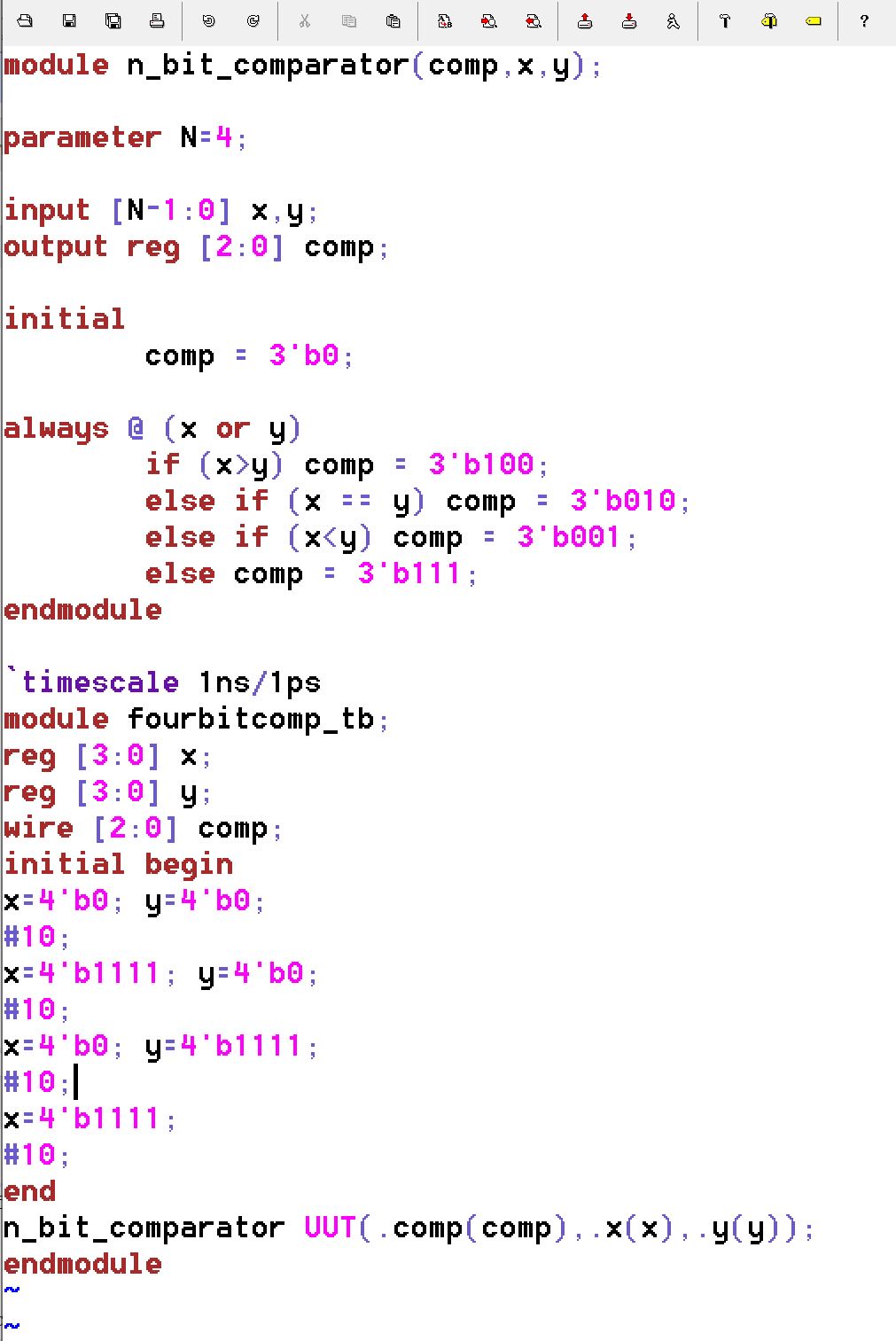
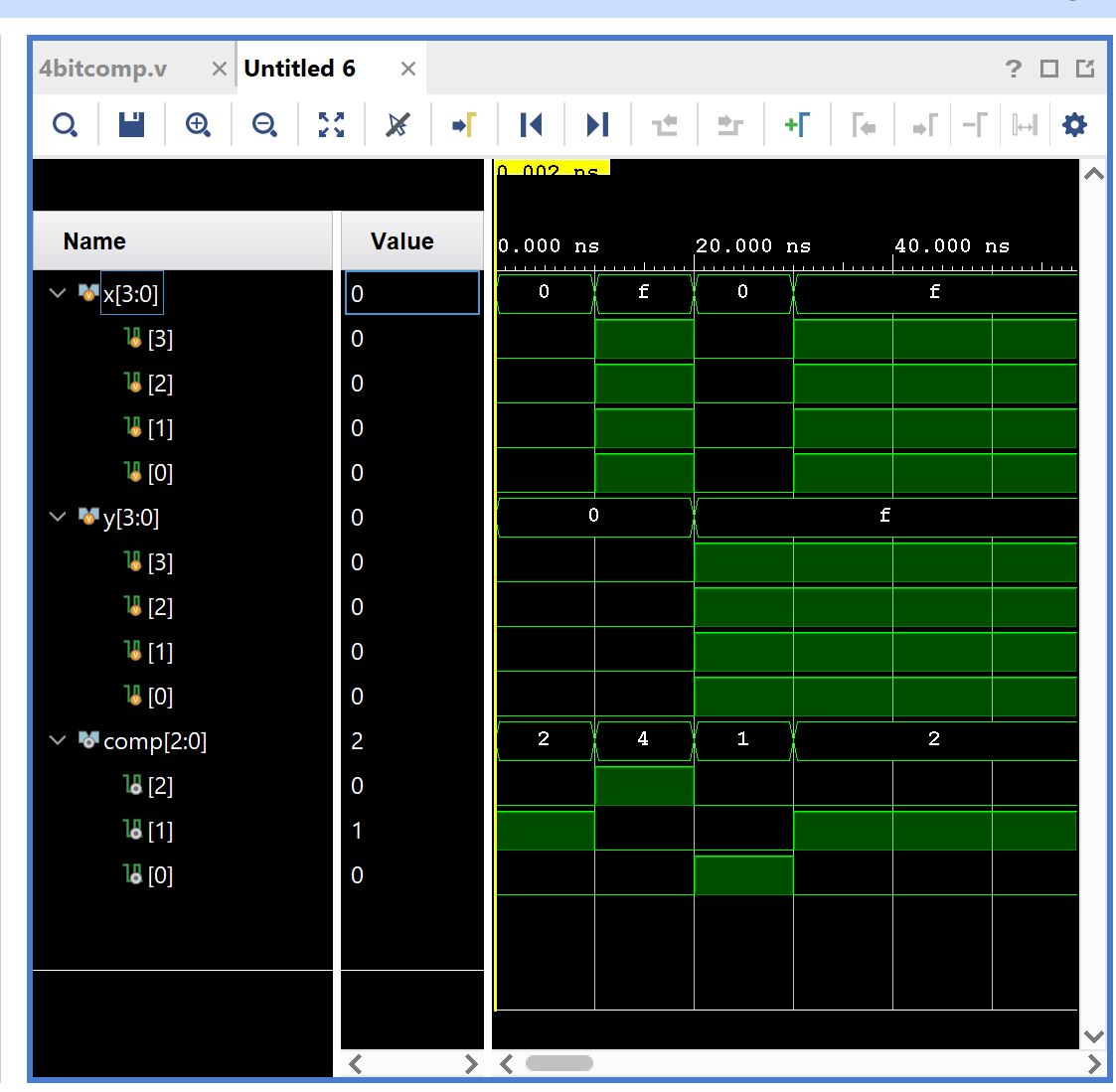
Task 3 In
this task we will be creating the test bench for the 4-bit comparator
example and verifying the functionality using a simulation in Vivado.
First we code the testbench and example in Verilog.
This can then be loaded into Vivado to run a simulation.
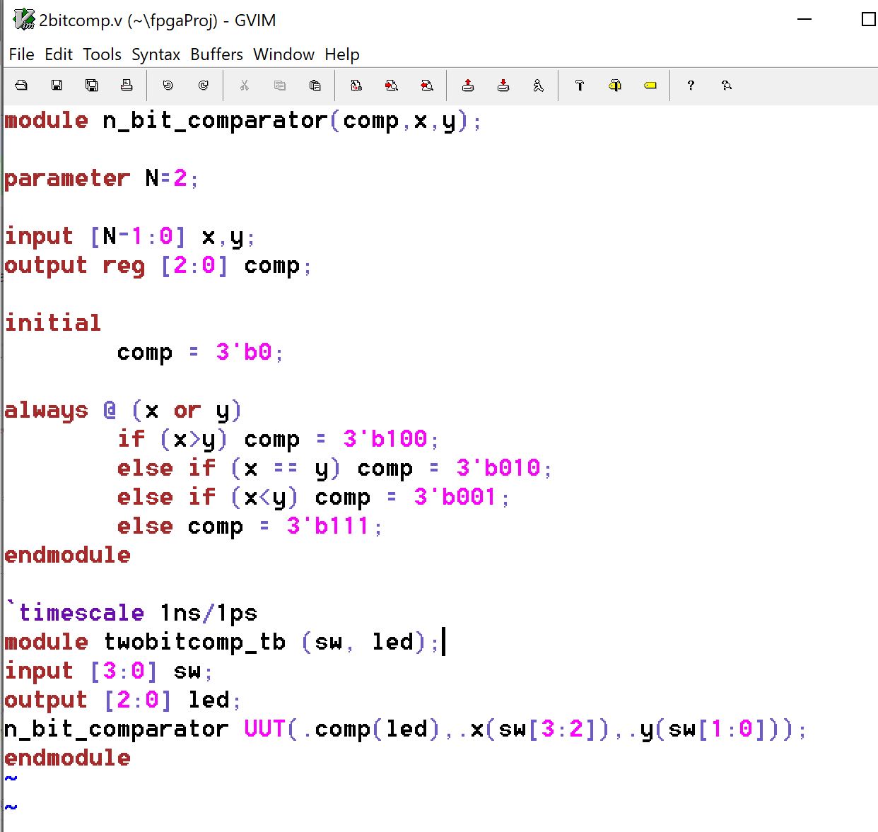
Task 4 In
this task we will create a 2-bit comparator for use on the FPGA board.
We will start by coding the comparator and the testbench in Verilog.
We can then upload the program to the FPGA.
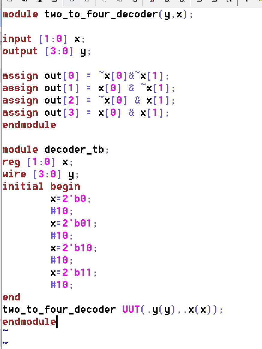
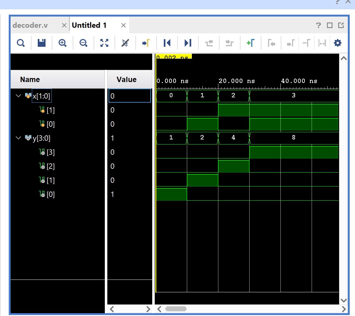
Task 5 In
this task we will be designing a testbench for a decoder using dataflow
modeling and verify the logic using a simulation. We first start by
coding the testbench and decoder example.
This can then be loaded into Vivado to run a simulation.
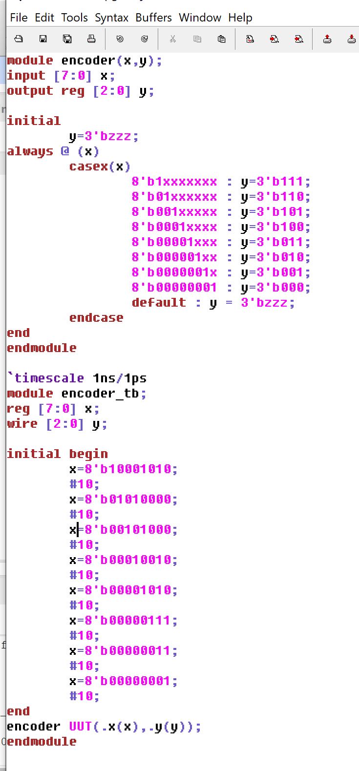
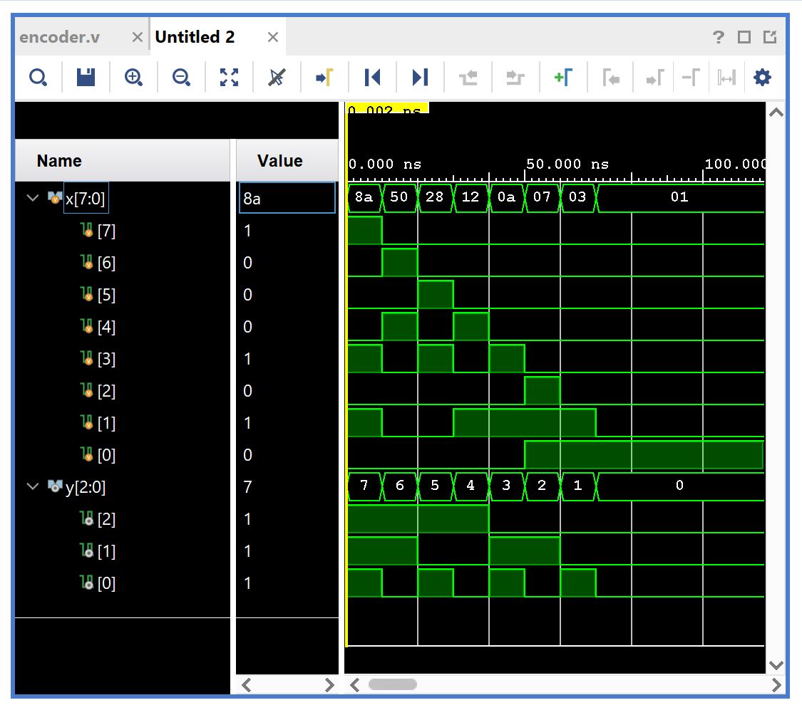
Task 6
In this task we will be designing a testbench for an 8x3 encoder and verify the logic using a simulation. We first start by
coding the testbench and decoder example.
This can then be loaded into Vivado to run a simulation.
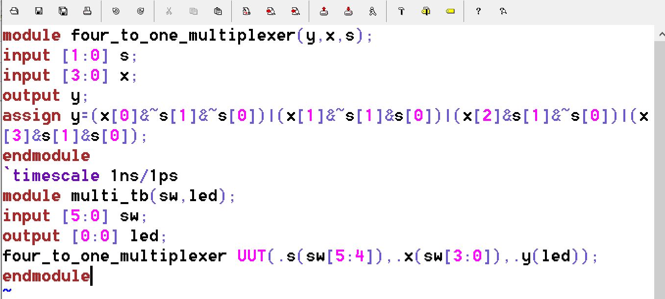
Task 7
In this task we implement a 4-1 multiplexer onto our FPGA board. Our program is first coded.
This program can then be uploaded to the FPGA board
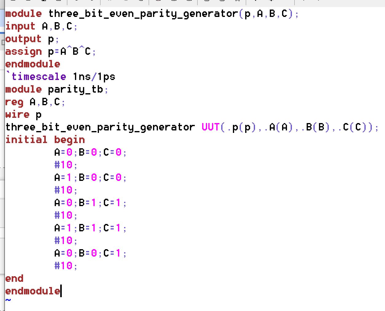
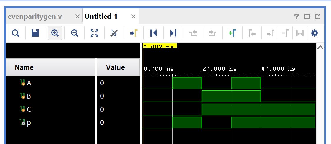
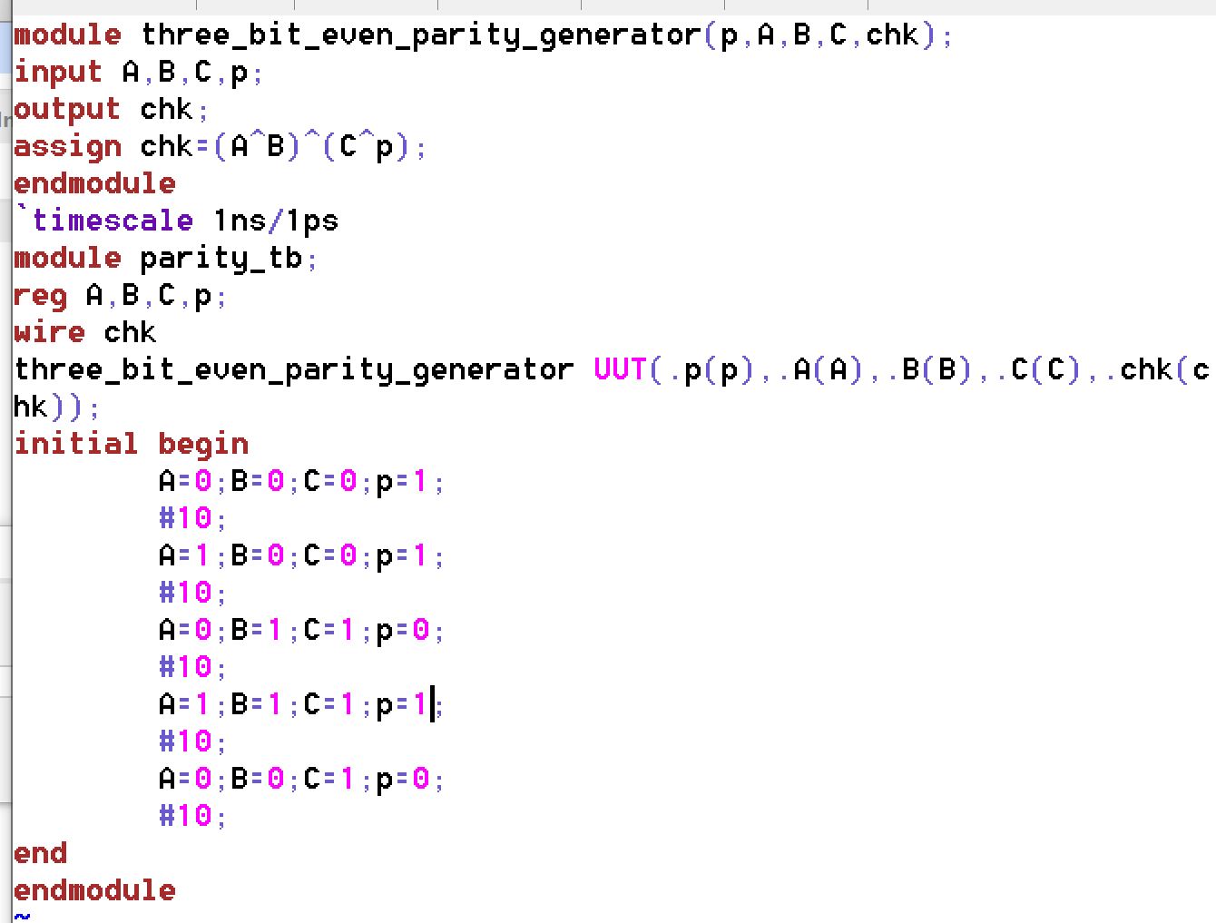
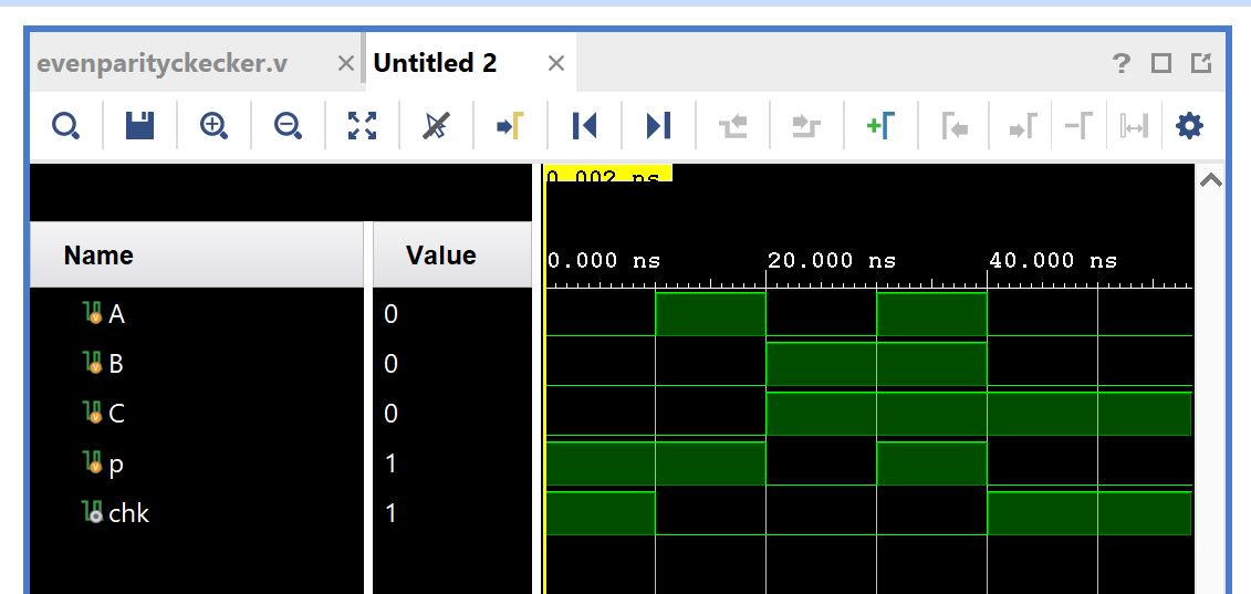
Task 8 In
this task we are instructed to design/verify and even parity generator
and checker in simulation. We will then implement the even parity
checker on the FPGA board.
First we make the even parity generator and then verify it via simulation.
Then we can do the same for the even parity checker.
Once this is complete we can create a new testbench and upload the checker to the FPGA.
Task 8
In this task we will implement the design of Section 8 and Section 9 onto our FPGA board.
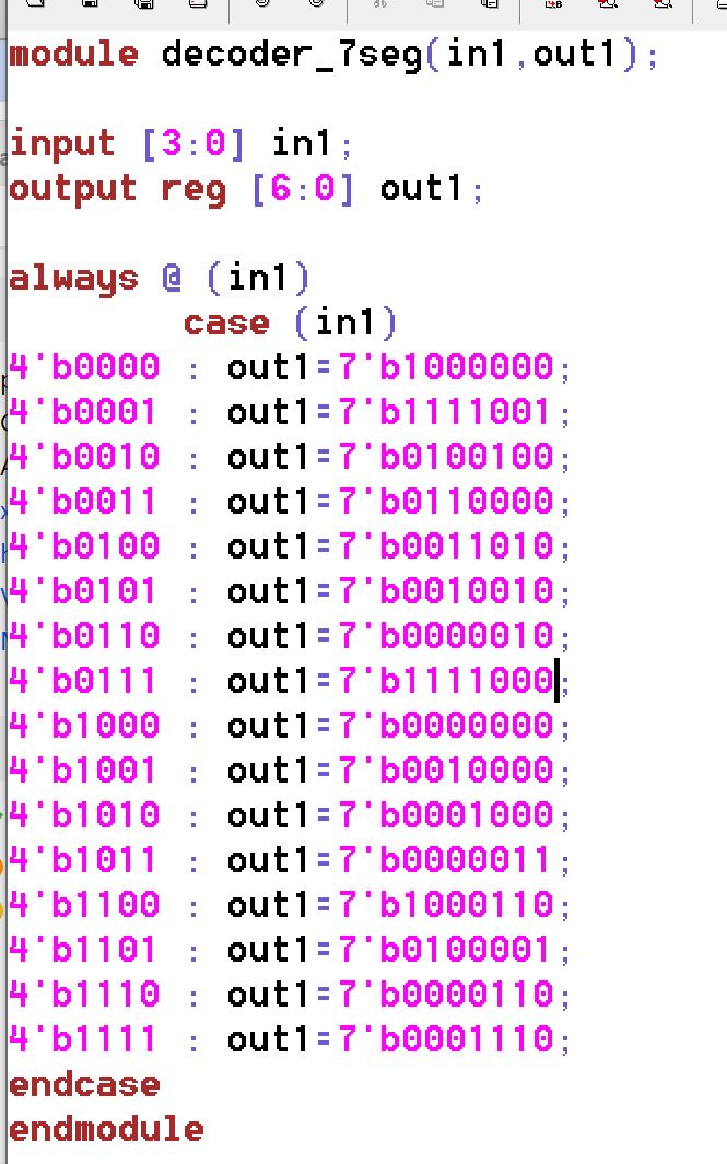
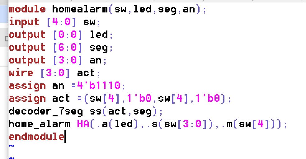
Section 8 This
section we will make an improved version of the home alarm task from
the previous tutorial. In this version when the system is armed the
seven segment display on the FPGA will switch from 0 to A.
First a decoder for the display is created
.
Then we can implement this with the previous example.
And finally we can upload the program to the FPGA to verify the functionality.
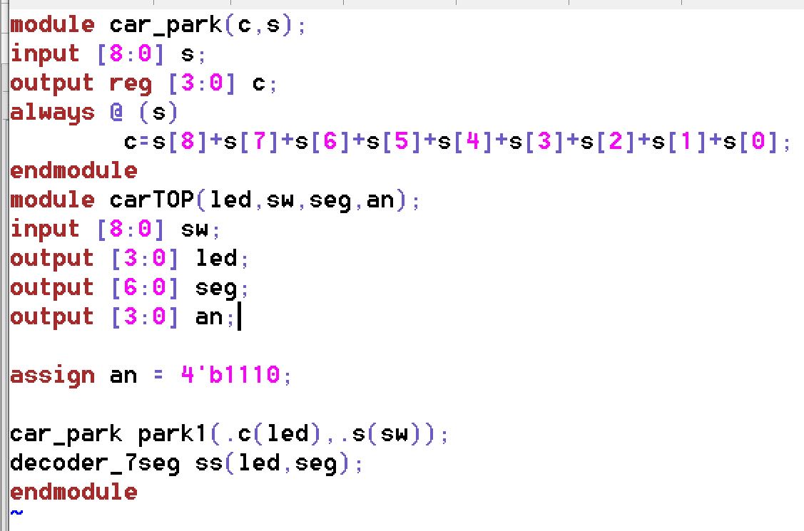
Section 9 This
section we will make a car parking spot counting system that counts the
total number of cars (switches on) in a parking spot and reports that
amount to the seven segment display. First this is coded in Verilog.
Now we can upload the program to the FPGA.
Discussion This
project is a great introduction into using combinational logic blocks
with Verilog as well as programming them onto the FPGA. This will be
useful when designing more complex systems that use these blocks to
function. This project was also a great introduction into the
seven-segment display feature on the FPGA.