CE433 2022 Spring
Lab 4
John Hitti
jdhitti@fortlewis.edu
Lab 4
Introduction
This Lab we will be working with programming combinational logic blocks and using them with our FPGA as well as simulations.
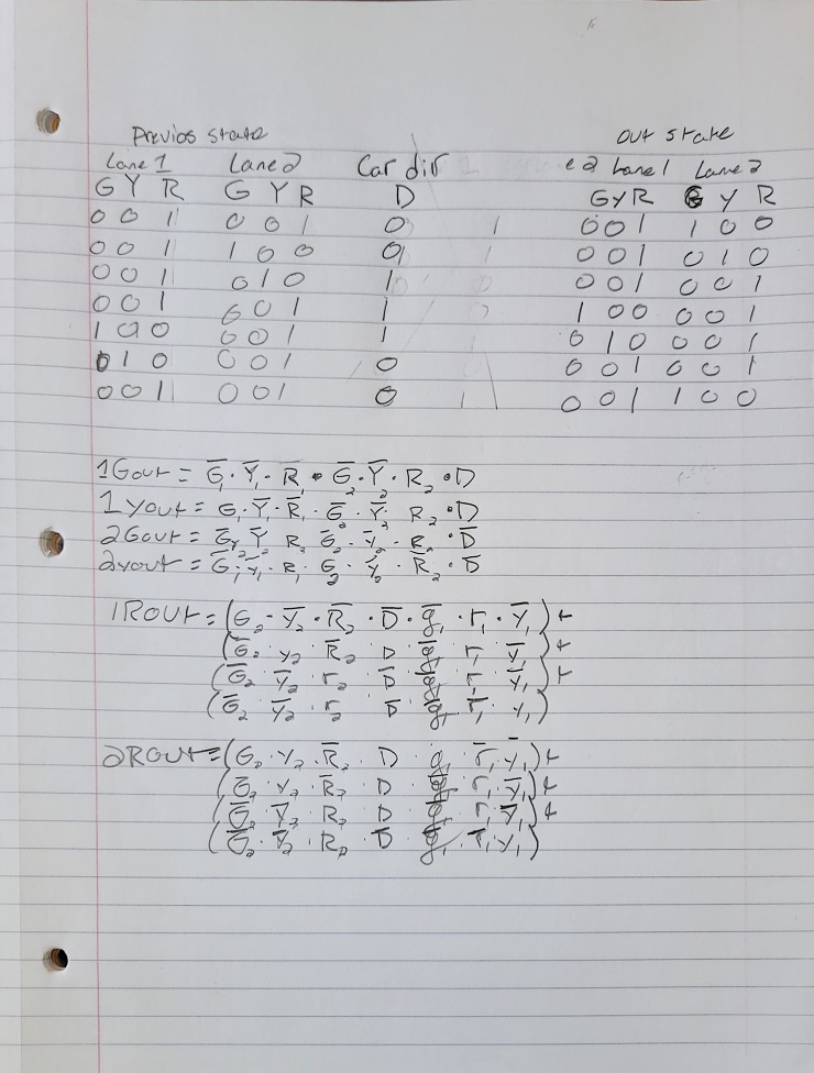
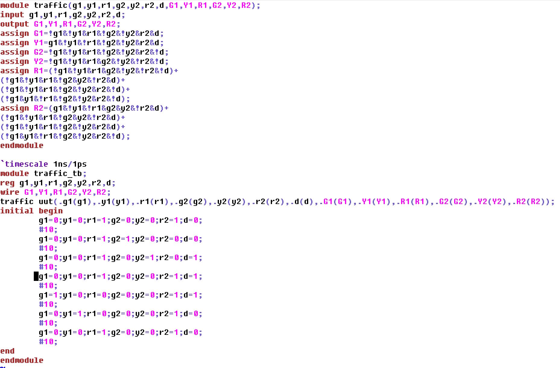
Task 1 In this task we
are instructed to draw a truth table for all the states for a two way
traffic light and derive the logic equations for this table.
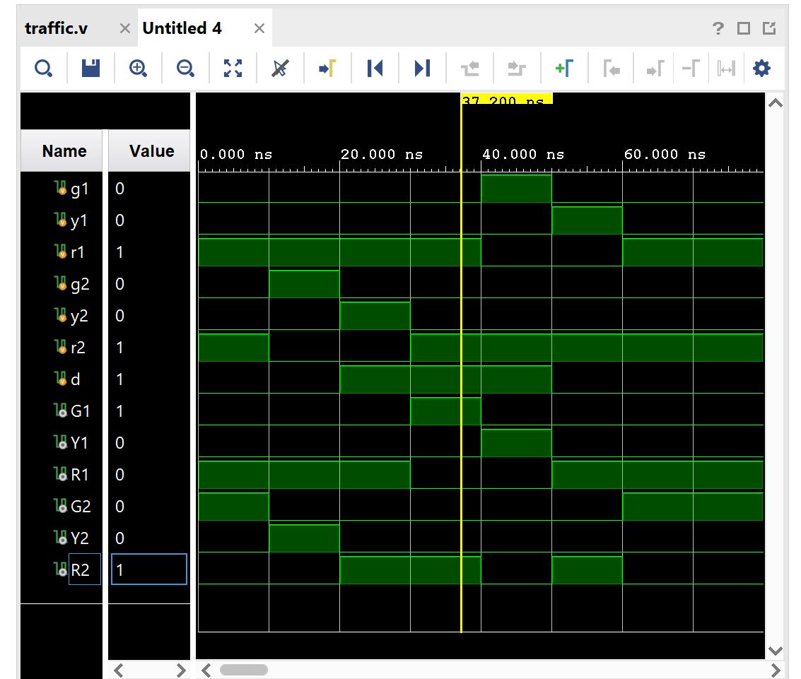
We can then design a Verilog model and a testbench for the simulation.
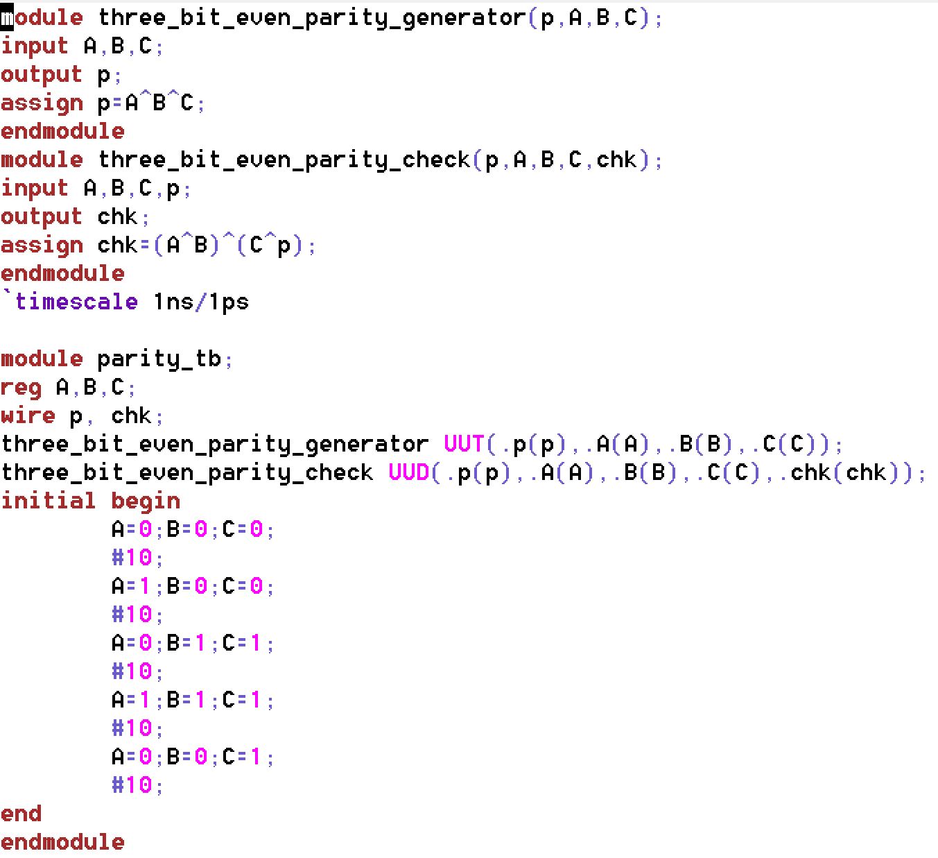
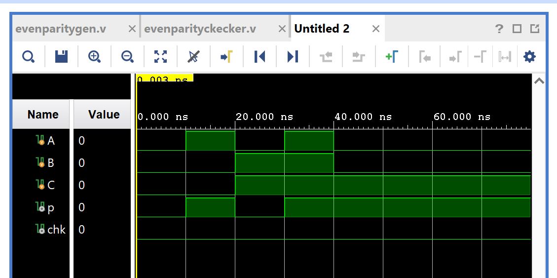
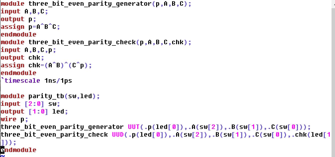
Task 2 In this task we will create an even parity generator (3-bit message with 1 parity bit)
and checker in Verilog and then connect. We will then connect the two
models and design a test bench to verify their functionality. First we
code the generator, checker and a testbench for simulation in Verilog.
A simulation can then be ran to verify functionality.
Once this functionality is verified we can create a testbench to upload our program to the FPGA.
Once this code is uploaded we can verify the functionality on the FPGA.
Discussion This
lab was an excellent introduction to using combinational logic blocks
with the FPGA as well as writing verilog code independently for a given
problem.