CE433 2022 Spring
Lab 3
John Hitti
jdhitti@fortlewis.edu
Lab 3
Introduction
This Lab we will be creating combinational logic blocks and uploading
them to our FPGA. We will also be creating and uploading programs to
utilize and familiarize ourselves more with the seven-segment display
and timing logic with the FPGA.
Task 1 In this task we
will be using Verilog and Vivado to demonstrate the following
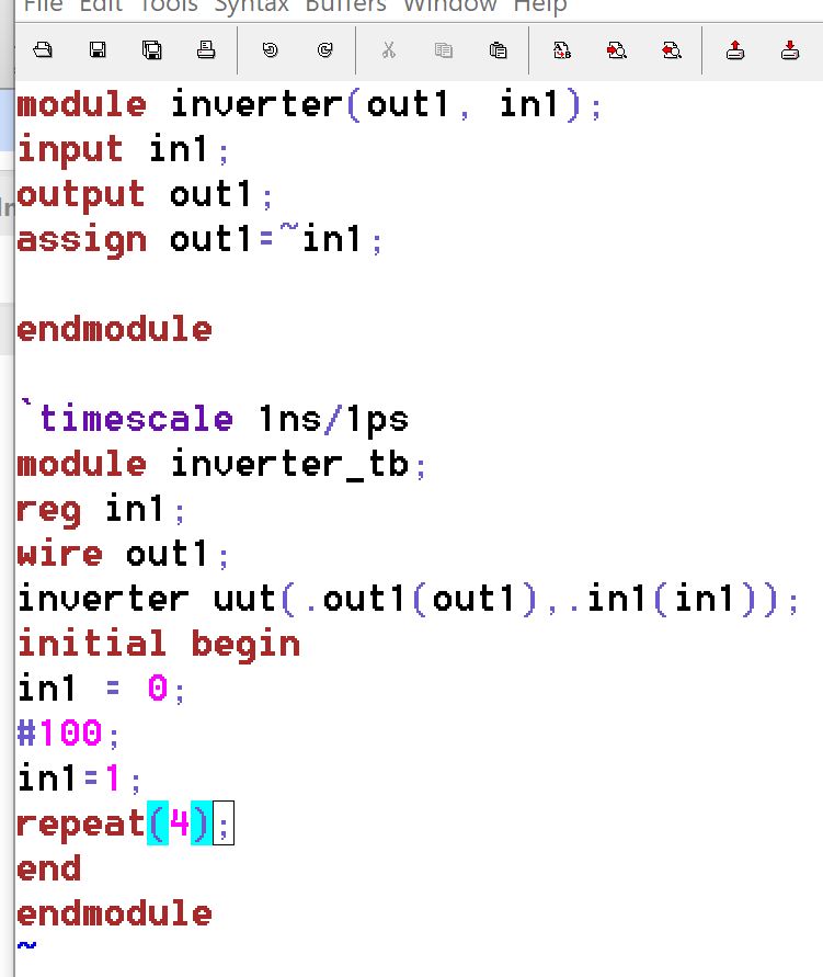
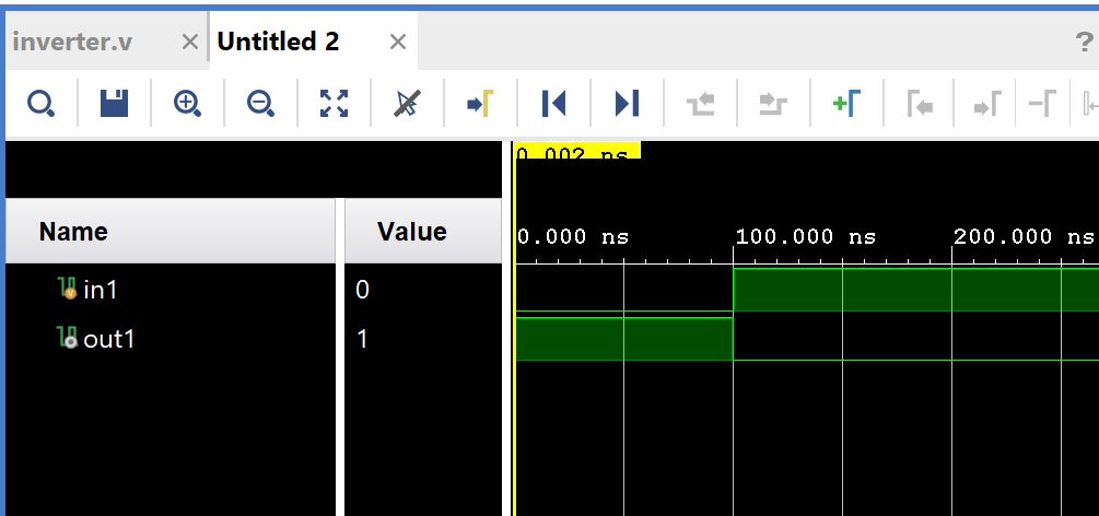
combinational logic blocks in a simulation an on our FPGA board. Inverter
First we start by coding the program in Verilog and running a simulation. Then we can verify the functionality on the FPGA.
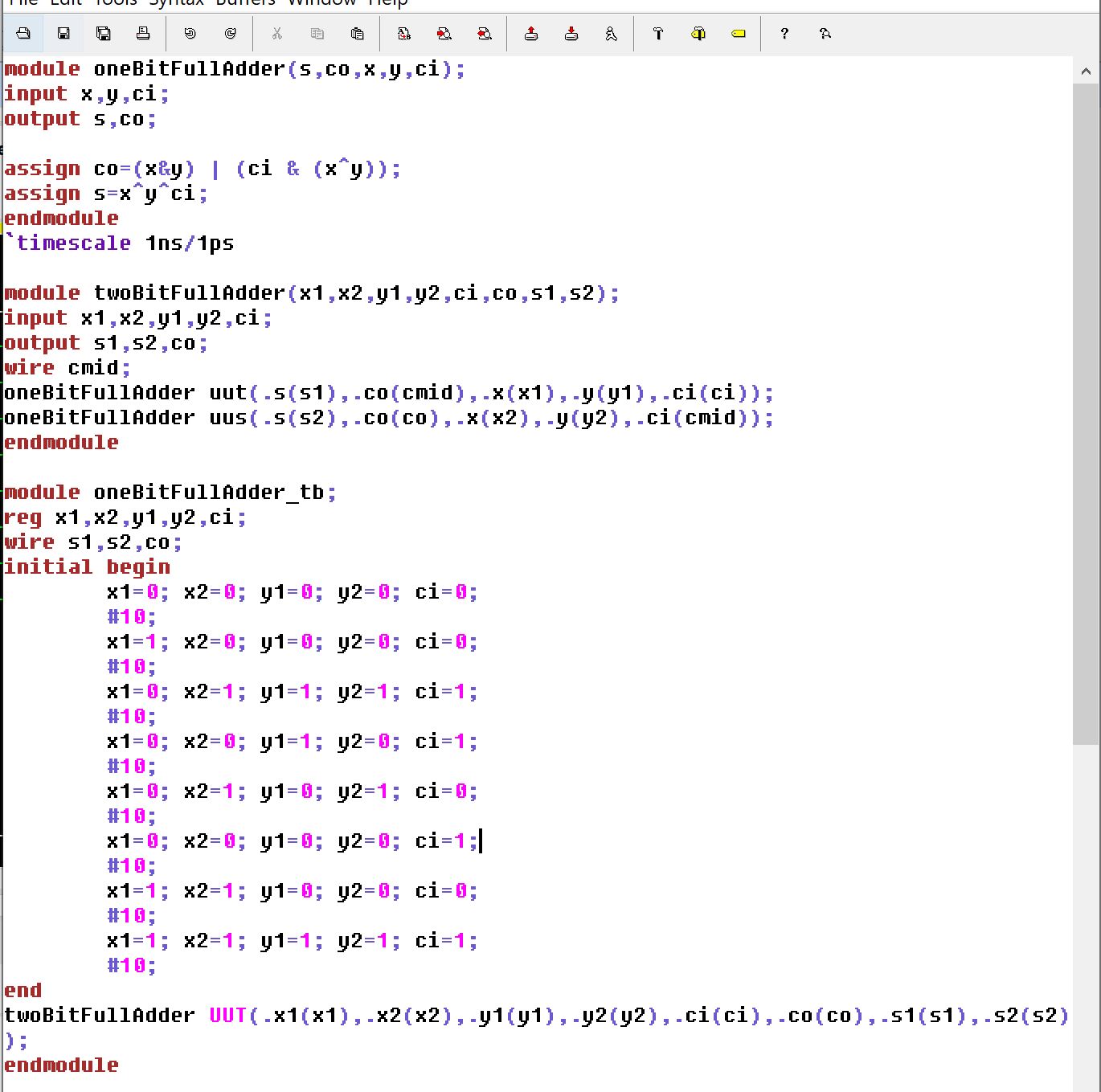
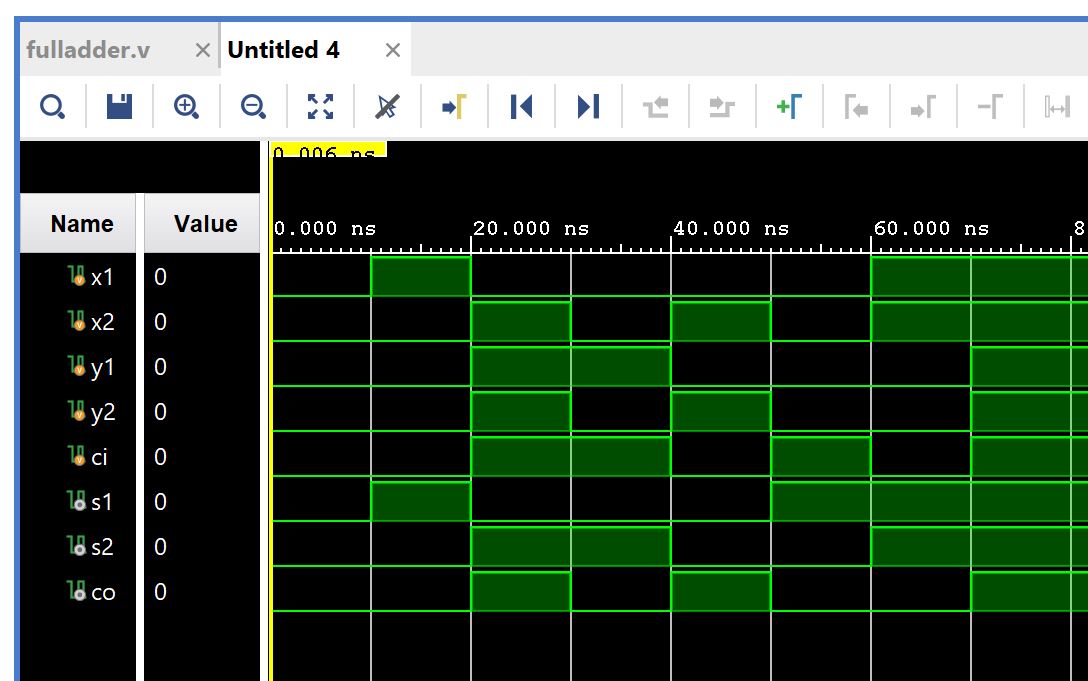
2-bit Full Adder
First we start by coding the program in Verilog and running a simulation. Then we can verify the functionality on the FPGA.
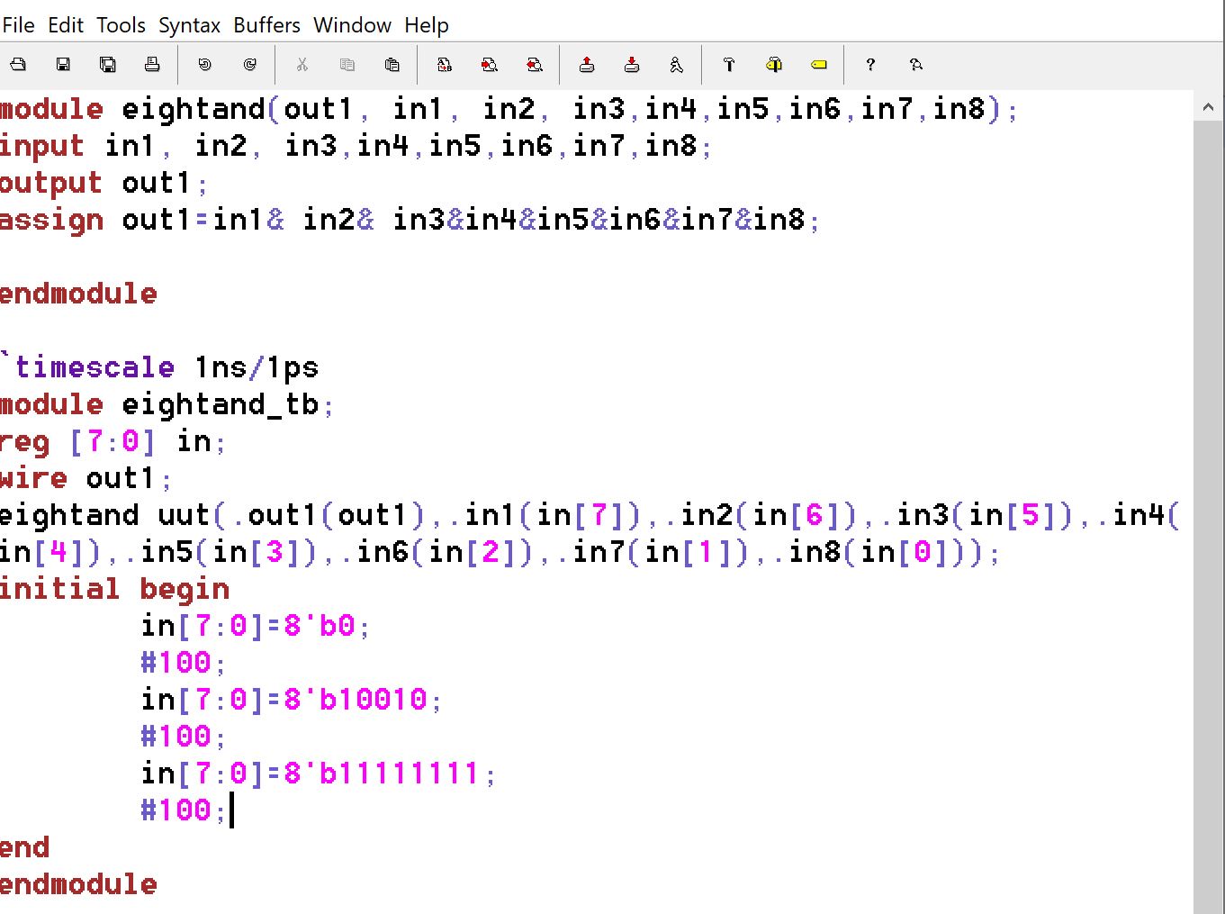
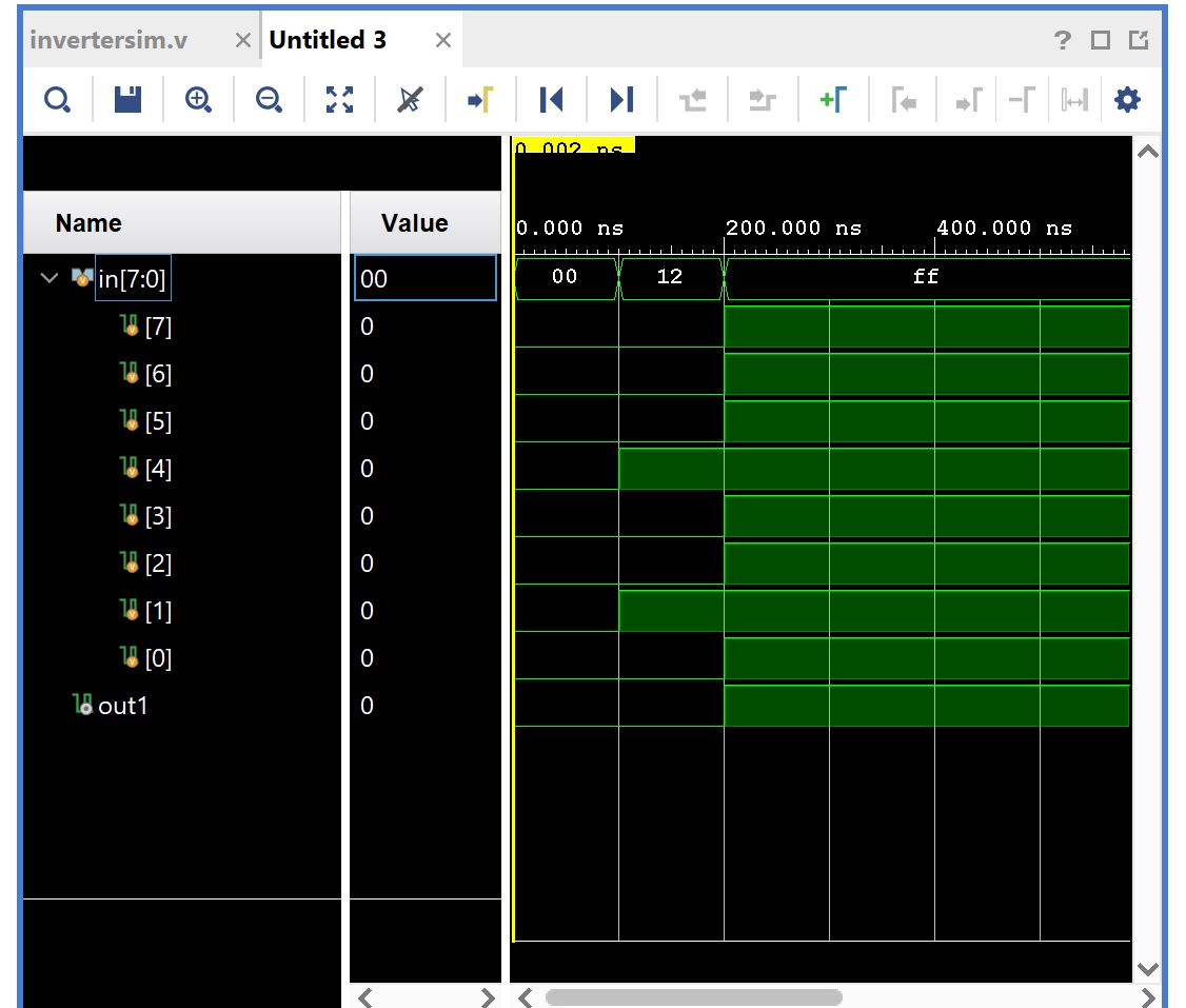
8-input And
First we start by coding the program in Verilog and running a simulation. Then we can verify the functionality on the FPGA.
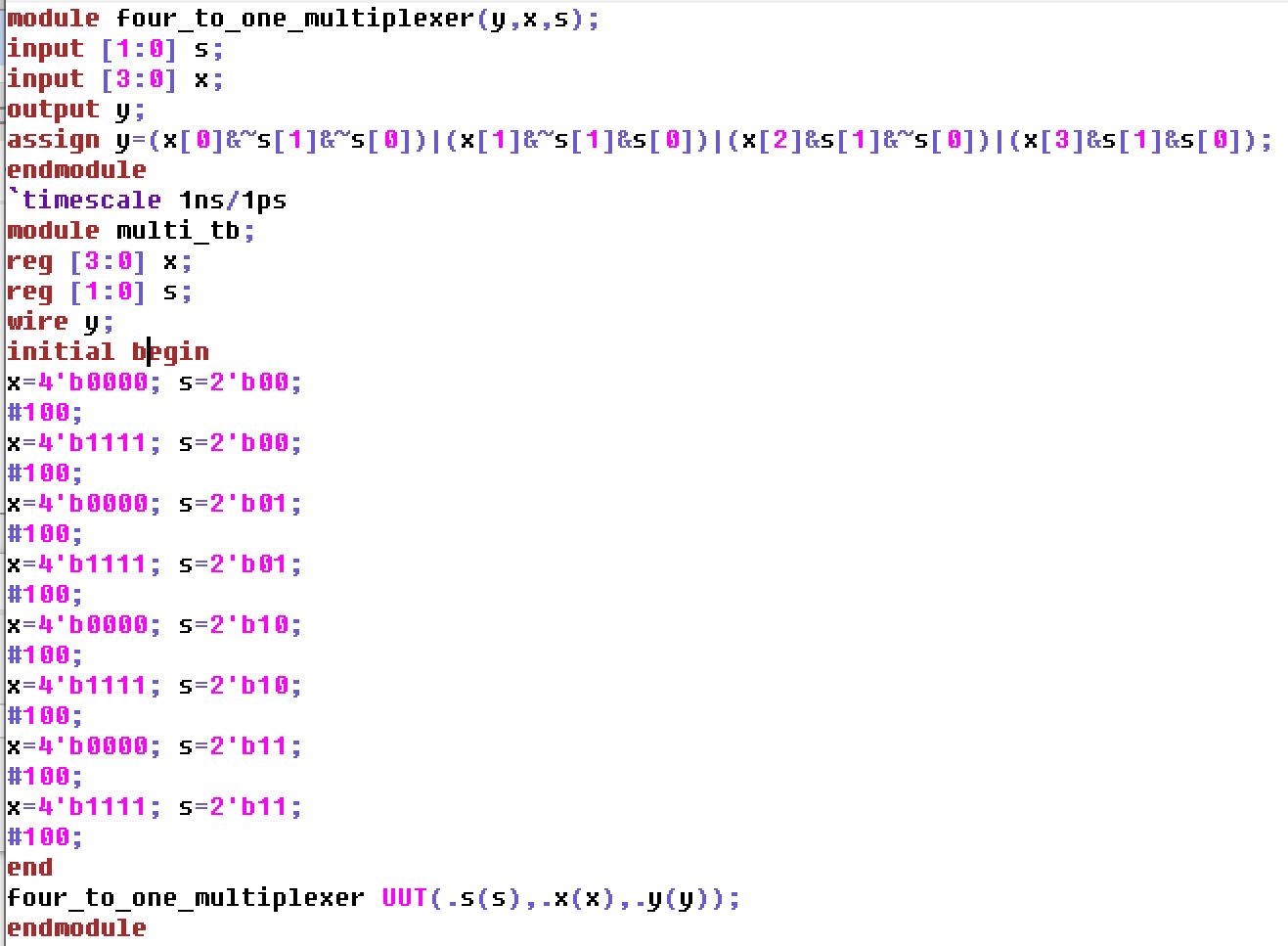
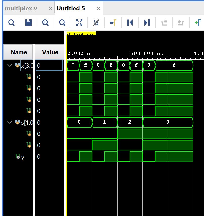
4-1 Mux
First we start by coding the program in Verilog and running a simulation. Then we can verify the functionality on the FPGA.
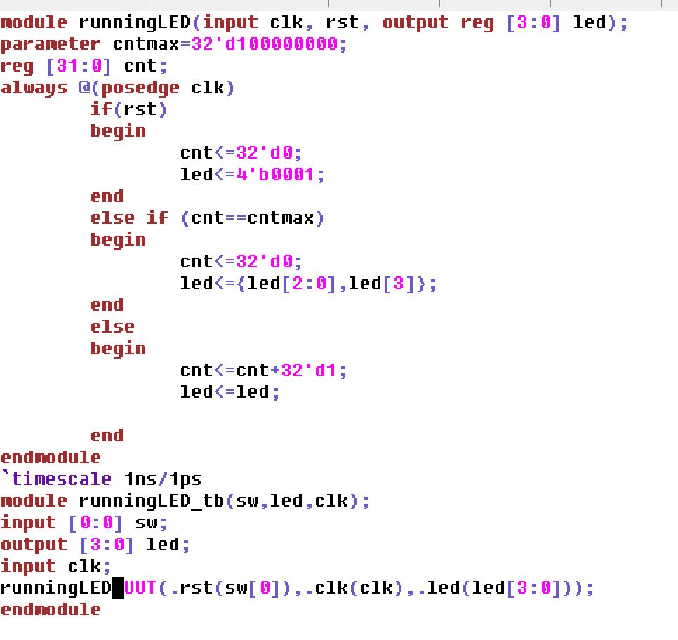
Task 2 In this task we
will use Verilog and Vivado to create a running led program in which a
segment of four LEDs take turns flashing on every second. First, we
create the program and testbench in Verilog and then we can verify the
functionality using our FPGA.
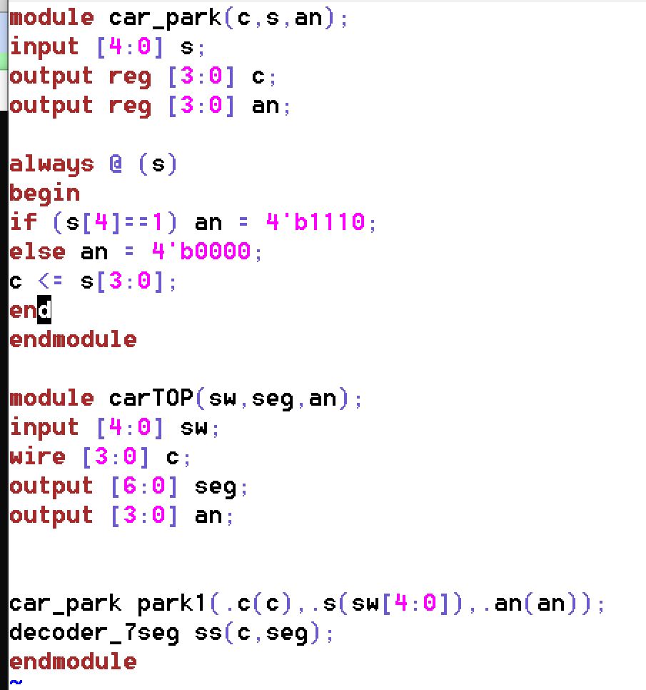
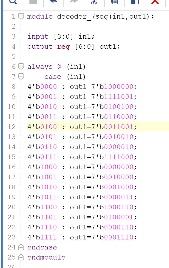
Task 3/4 In this task we
will create a program that will take a binary number (0 to 9) and
display it to the whole seven-segment display. There will also be an
option to only display the output on part of the seven-segment display.
First, we will create the code in Verilog and then we can upload it to
our FPGA.
Discussion This
lab was an excellent introduction to more complicated combinational
logic blocks and using them with the FPGA. This lab also helped to make
us more familar with the seven-segment display onboard our FPGA.