ENGR338 Lab Spring 2021
Lab 8: Design a MUX, and a High-Speed Full Adder
Name: Audra Benally
Email: albenally1@fortlewis.edu
1. Title: Design a MUX and a High-Speed Full Adder
2. Introduction: In this 2 week lab, we built a MUX in schematic
and layout view. Then the MUX was used to make an 8bit MUX in schematic
and layout as well. Afterwards we built a Full Adder modeled in Dr.
Baker's CMOS book. This adder uses AOI logic to cut down on the
components needed in the layout. Because it is a smaller design it is
much faster than the last full adder we built. After the high speed
Full Adder was built in schematic and layout view, an 8bit version was
made using this design.
3. Materials and Methods:
Materials:
- Computer
- Computer Mouse
- LTSpice Software
- ElectricVLSI Software
Methods:
For this lab,
we started by building a MUX. My 1bit MUX was already
made from a HW3 assignment so I was able to start with building the
8bit MUX. The MUX was made in schematic and layout view. Figure 2 shows
the DRC, NCC, and well check results of the finished 8bit MUX. The 8bit
MUX was then simulated successfully with the results shown in Figure 3.
After the MUX was done, a 1bit full adder was made from Dr. Baker's AOI
logic in the CMOS book. Figure 4 shows the schematic while figure 5
shows the layout view. The layout was carefully made with DRC checks
all along the way. I tried not to copy the lab so my layout was very different than what was online. I
used a lot of Polysilicon and Metal1 for my design. The final design
passed DRC, NCC, and well checks as seen in figure 5. The 1bit full
adder was then simulated to make sure it worked properly. Results of
this sumulation can be seen in figure 6. In the last task the 1bit Full
Adder was used to make an 8bit full adder. The schematic can be seen in
figure 7. The layout passed all DRC, NCC, and well checks and can be
seen in figure 8. Finally, the 8bit Full Adder was simulated with the
results shown in figures 9, 10, and 11.
4. Results:
~ Task 1 : MUX (1bit and 8bit)
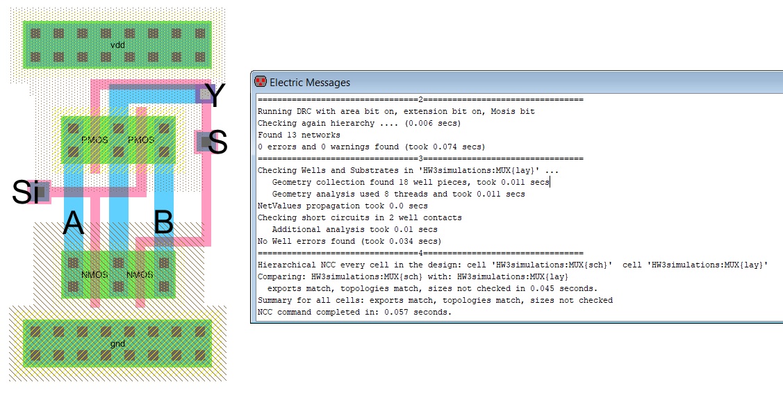
Figure 1. 1bit MUX with clean DRC, NCC, and well checks.
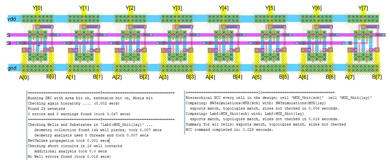
Figure 2. 8bit MUX with clean DRC, NCC, and well checks.
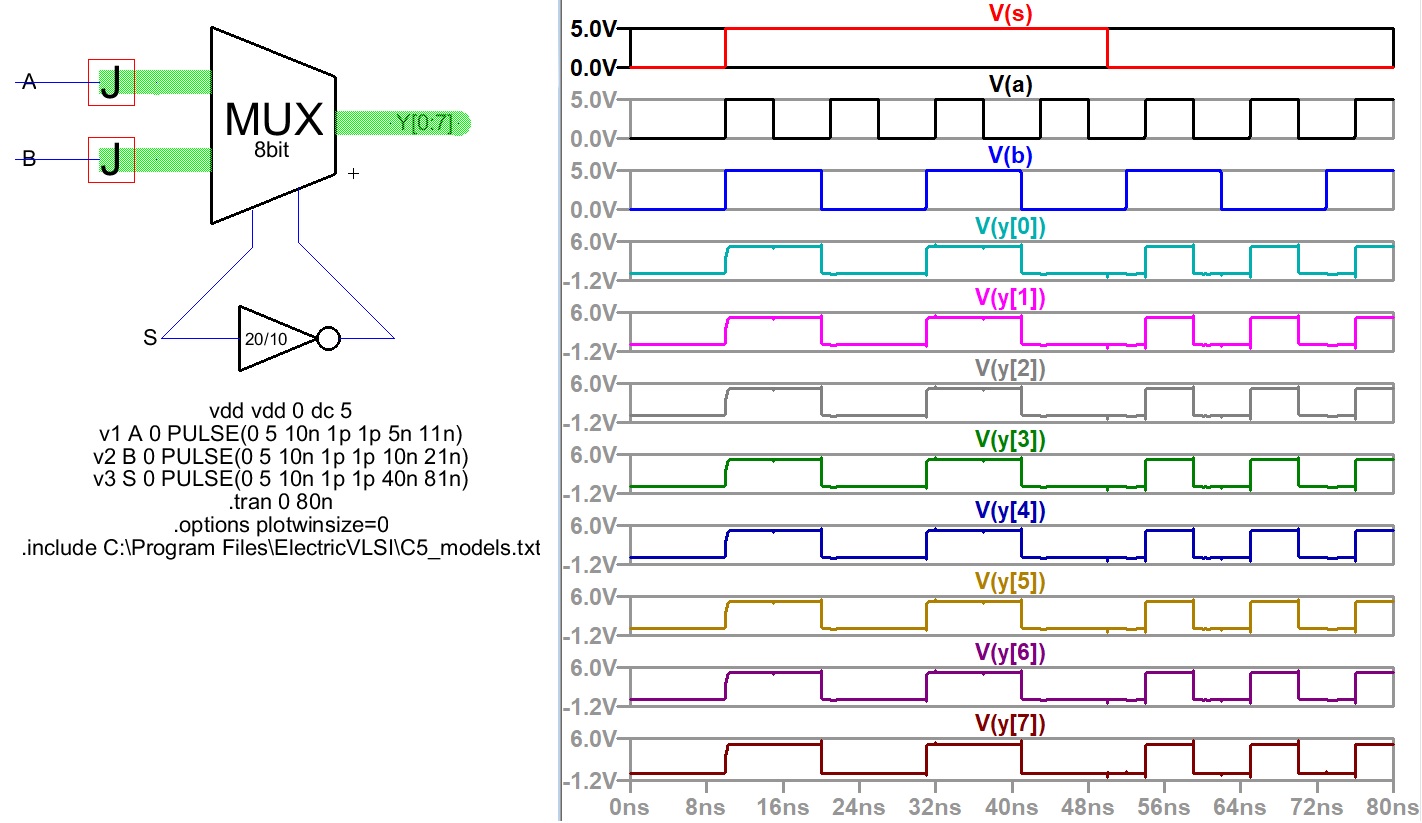
Figure 3. 8bit MUX simulation.
~ Task 2: 1bit High-Speed Full Adder
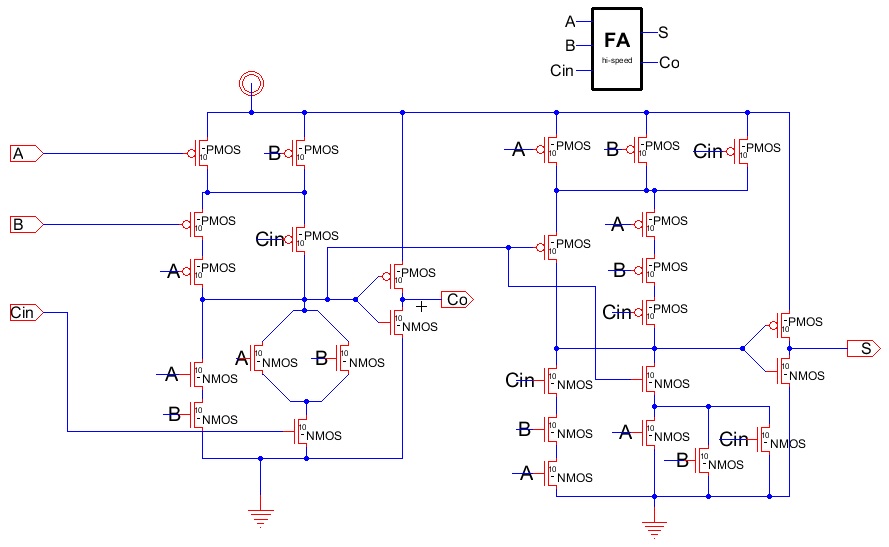
Figure 4. High speed Full Adder schematic
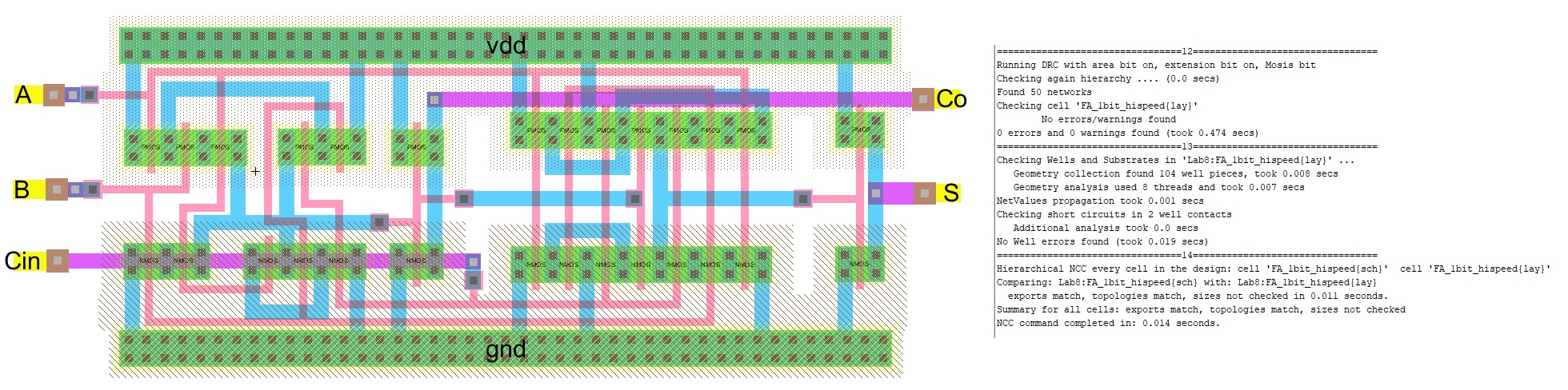
Figure 5.
1bit Full Adder layout view with DRC, NCC, and well check results.
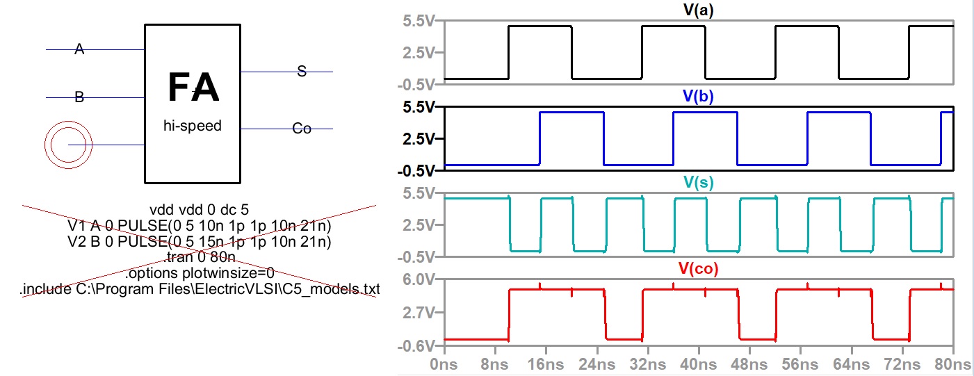
Figure 6. 1bit Full Adder simulation results.
~ Task 3: 8bit Full Adder
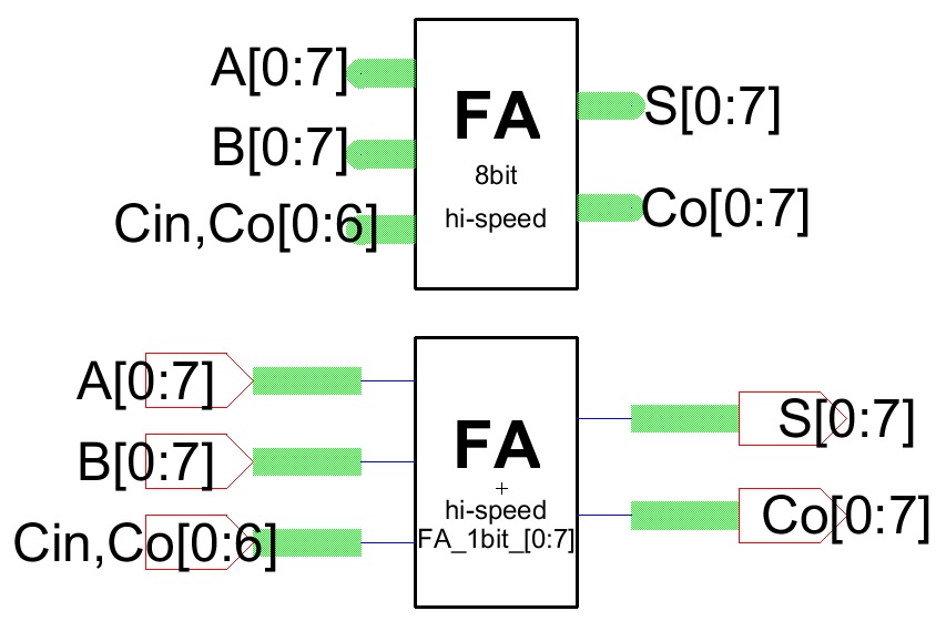
Figure 7. 8bit Full Adder schematic (bottom) and icon (top) view.
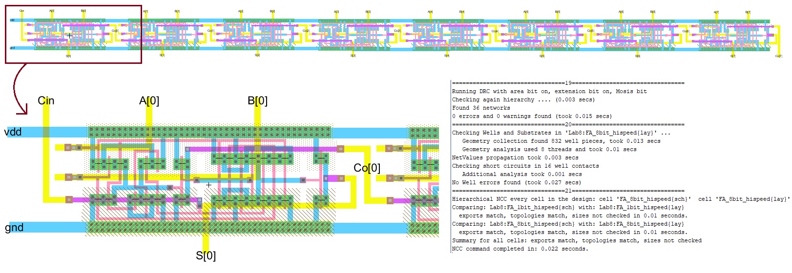
Figure 8.
Finished 8bit Full Adder layout with DRC, NCC, and well checks.
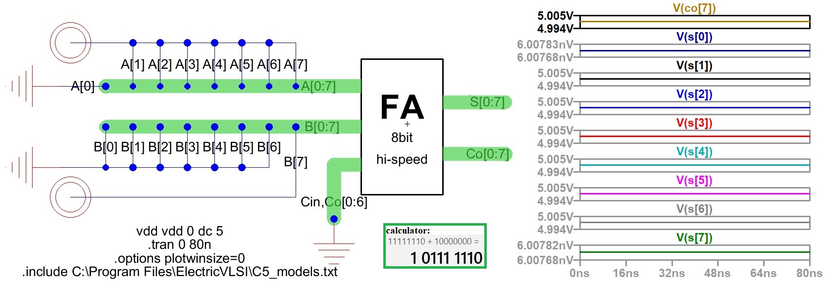
Figure 9.
First 8bit Full Adder simulation using what was suggested in the lab.
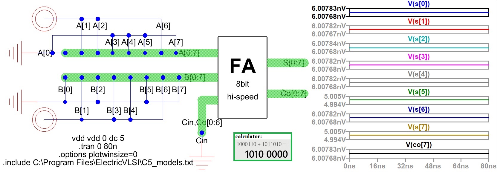
Figure 10.
Second 8bit Full Adder simulation. Calculations are shown in the green
box.
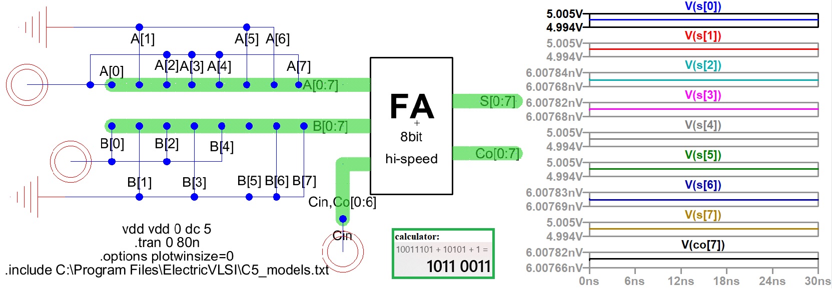
Figure 11.
Third 8bit Full Adder simulation. Calculations are also in the green
box.
5. Discussion
This lab was really enjoyable. I was super happy when I realized I
already had a head start because of what I had gotten done for HW3. I
think I had more trouble with the schematic of the high speed full
adder than the layout. What I had from HW3 had a lot of wires all over
the place that I replaced with the wire naming method. I still really
enjoy putting the layouts together and making them match the
schematics. This time around I tried to not look at/copy the layout
online and make the design myself based on my schematic. The only
mid-layout changes I had to make were to reverse the order of the "A,
B, Cin" on the bottom left corner of the "S" portion of the schematic
so that the layout would fit better. I was also a little unsure about
my layout design since it is really different than what is online. I
used a lot of Poly and Metal1 to connect most of the gates and
connections. I'm pretty sure the metal to avoid was the purple Metal 2
for added resistance reasons. I don't remember if Poly or Metal 1 had
similar issues. Other than that the lab went great!