ENGR338 Lab Spring 2021
Lab 7: Using Buses in ElectricVLSI
Name: Audra Benally
Email: albenally1@fortlewis.edu
1. Title: Using Buses in ElectricVLSI
2. Introduction: In this 2 week lab, we built several 8bit logic
gates using buses and the gates that we built in the last lab. The
first was a ring oscillator that is built from 11 inverters in series.
The second was the 8bit AND gate, then the 8bit OR gate, followed by
the 8bit NAND then the 8bit NOR gate. All of these gates were simulated
then created in the layout view. All of the simulations were successful
and all of the layouts were cleared with NCC, DRC, and the well check
tests.
3. Materials and Methods:
Materials:
- Computer
- Computer Mouse
- LTSpice Software
- ElectricVLSI Software
Methods:
For this lab,
we built 8bit logic gates using buses and the array naming system.
For the ring oscillator, first 11 inverters were connected in series in schematic view and one
of the outputs was marked as "osc_out". Then the ring oscillator was
recreated in a second schematic with the buses. The inverter outputs were connected to bus
wires and 10 in's were connected to 10 outs, plus osc_out, using the array naming
system. The schematic with the buses was simulated, see Figure 1., to
make sure it was reacting in the way it should. The ring oscillator was
then made in layout view using a short inverter. All of the outs were
exported and the layout passed DRC, NCC, and well checks as seen in
Figure 2. Task 2 and Task 3 were very similar in that they were both
had to prep their logic gates using the Lab 6 schematics of the NAND or
NOR gates paired with an inverter. The icons were then used to make the
8bit versions of the gates. This was made using buses again and the
array system: [0:7] for the A and B inputs as well as the AandB or AorB
outputs. Each gate was simulated before the layouts were created using
the layouts from Lab 6 with each output and input labeled each bit from
0 to 7. Tasks 4 and 5 were made in the same way except their gates were
already made from Lab 6. All the gates passed the DRC, NCC, and well
check tests and all the simulations acted as expected.
4. Results:
~ Task 1 : Ring Oscillator
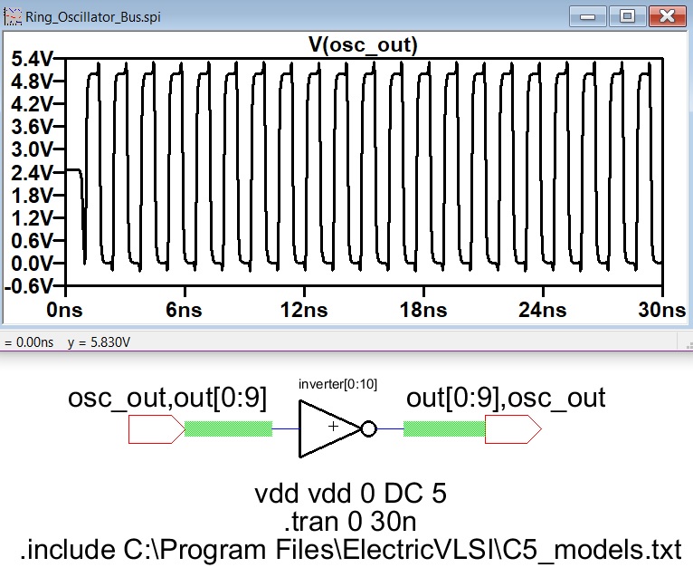
Figure 1. Ring Oscillator made using buses.
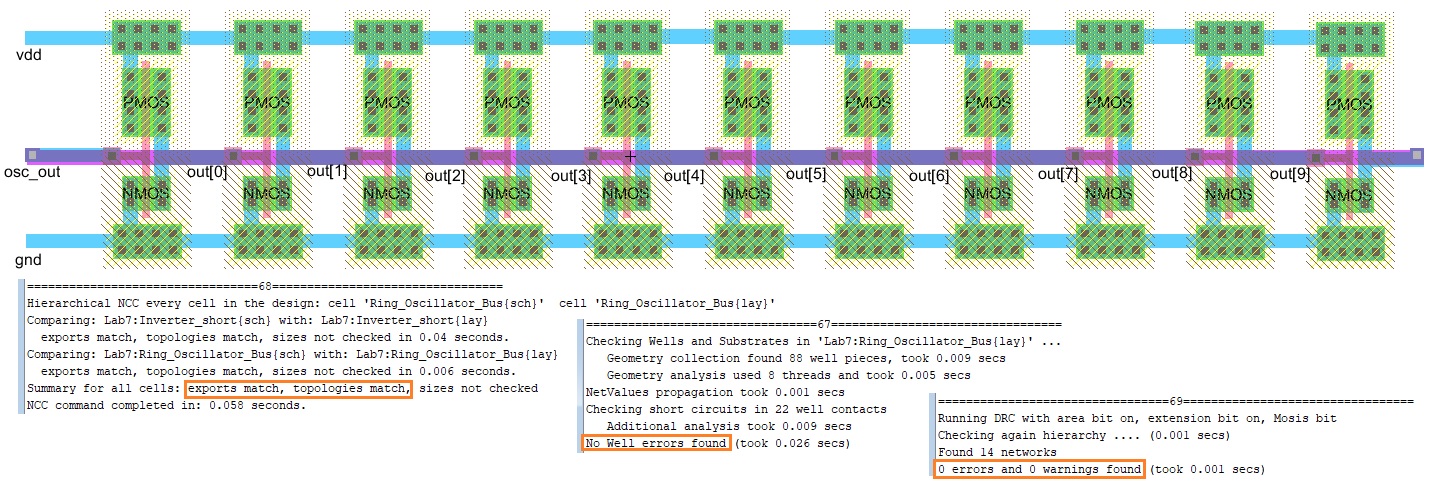
Figure 2. Finished ring oscillator layout.
~ Task 2 : 8bit AND gate
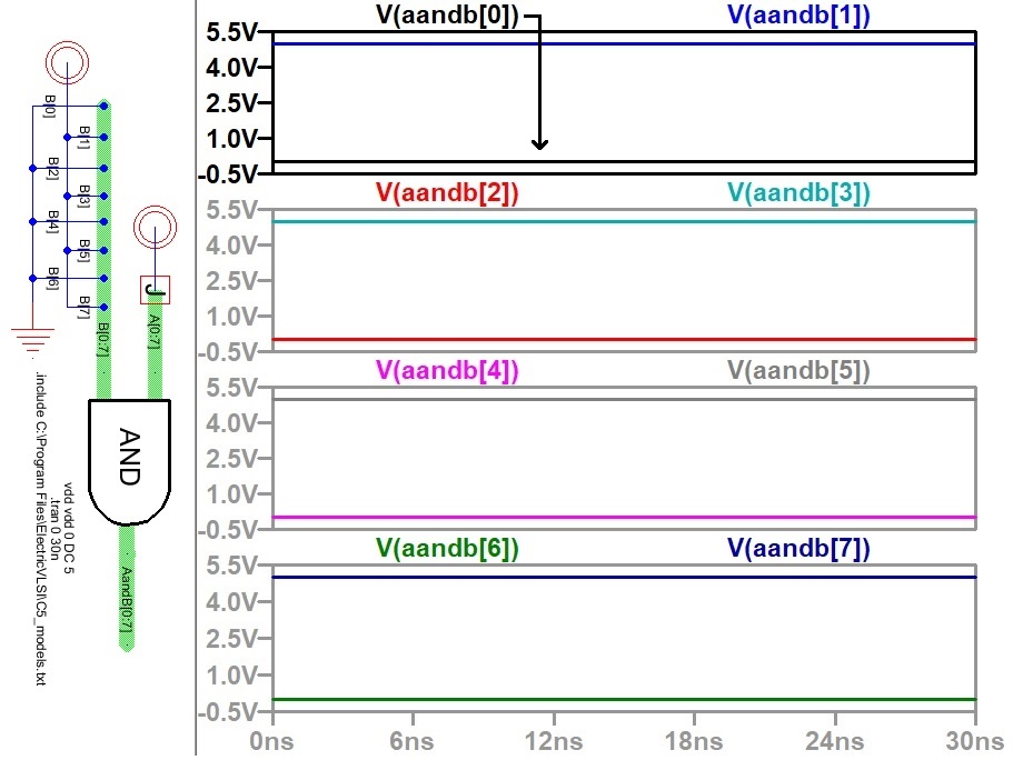
Figure 3. AND gate simulation results with A connected to vdd.
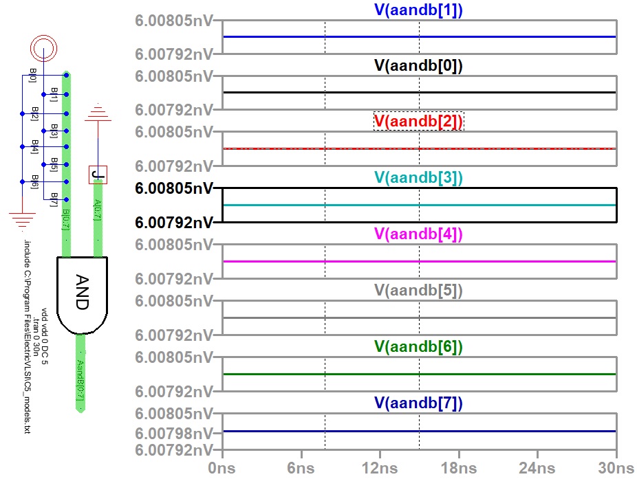
Figure 4. AND
gate simulation results with A input connected to gnd.
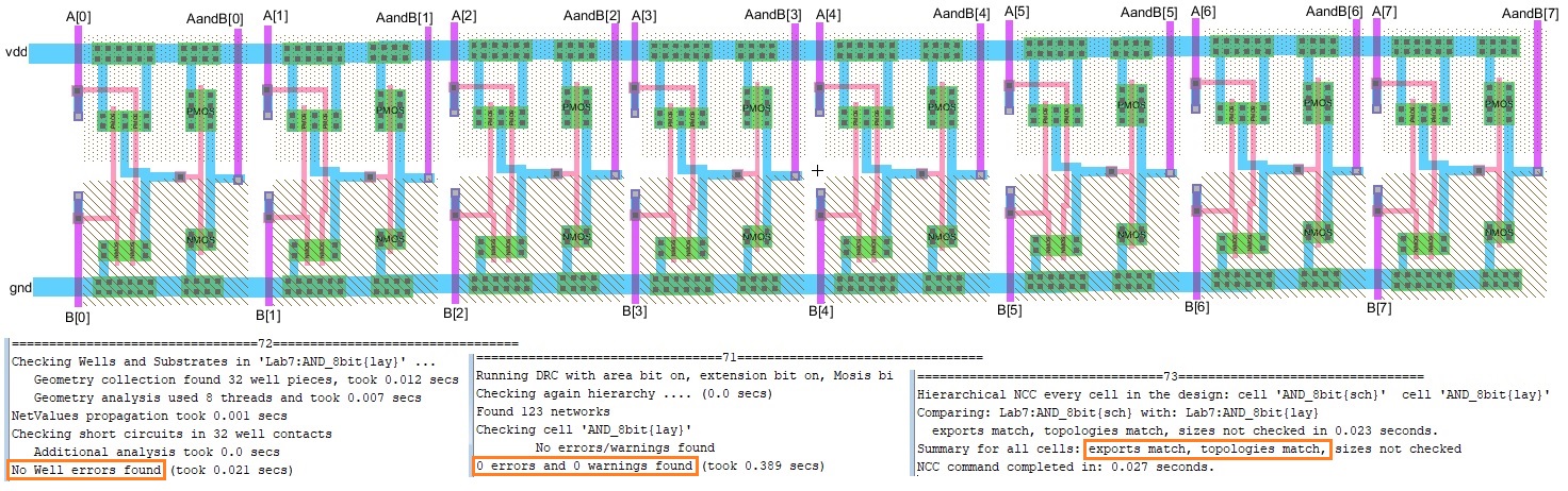
Figure 5. Finished AND gate layout.
~ Task 3 : 8bit OR gate
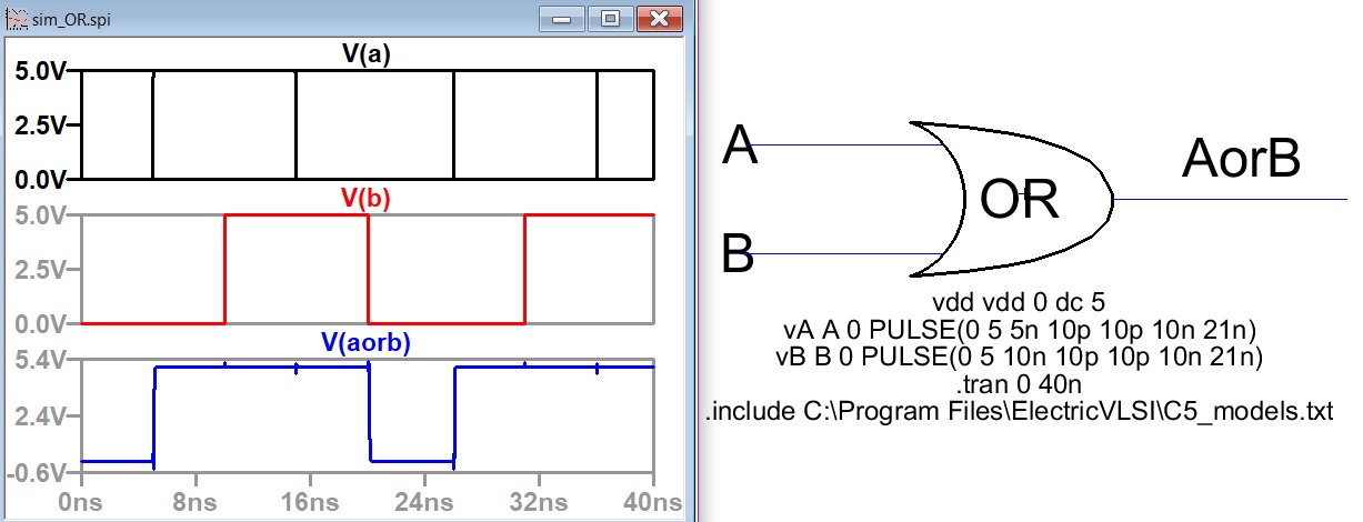
Figure 6. OR gate simulation to make sure it is correct.
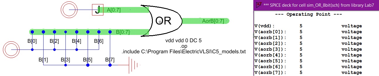
Figure 7.
8bit OR gate simulation with the buses attached to different signals.
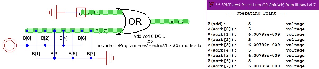
Figure 8.
8bit OR gate simulation #2 to better show the OR gate logic.
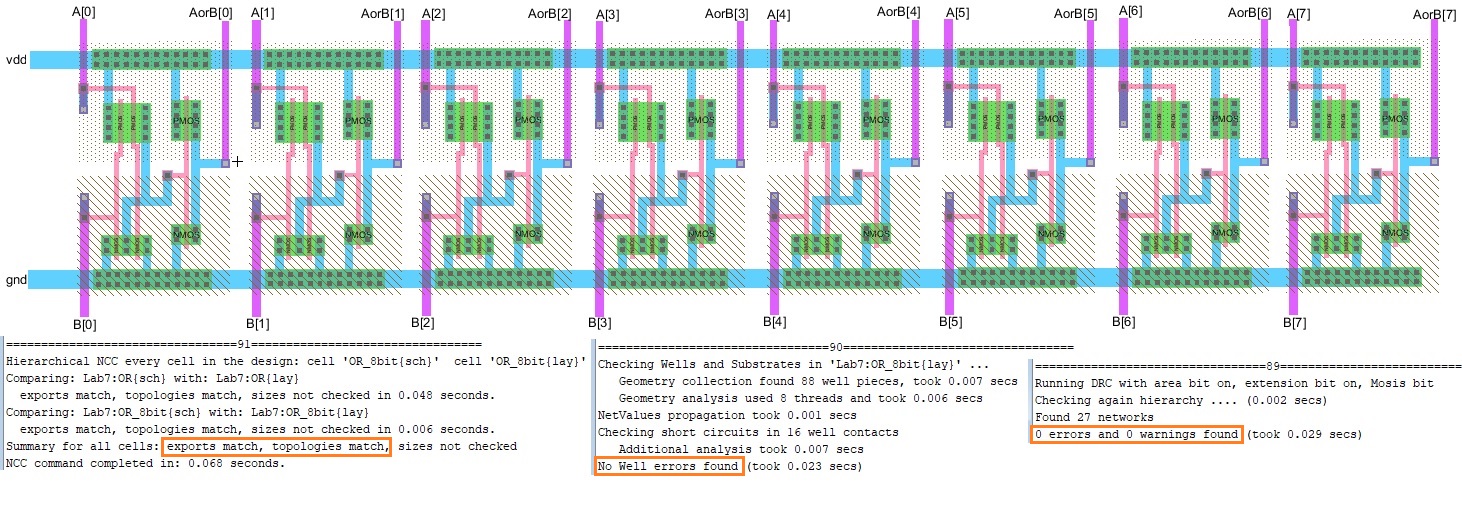
Figure 9. Finished 8bit OR gate layout.
~ Task 4 : 8bit NAND gate
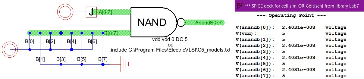
Figure 10. 8bit NAND gate simulation #1.
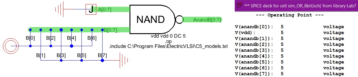
Figure 11. 8bit NAND gate simulation #2.
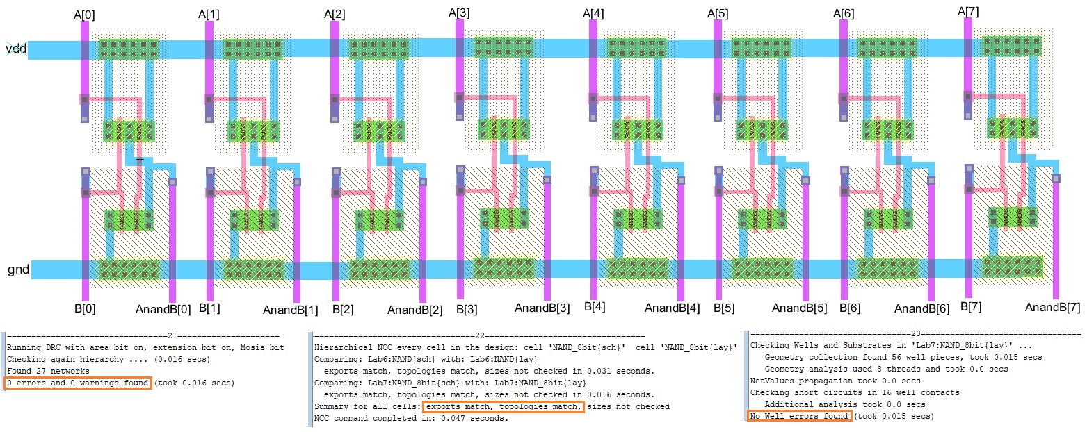
Figure 12. Finished 8bit NAND gate layout.
~ Task 5 : 8bit NOR gate
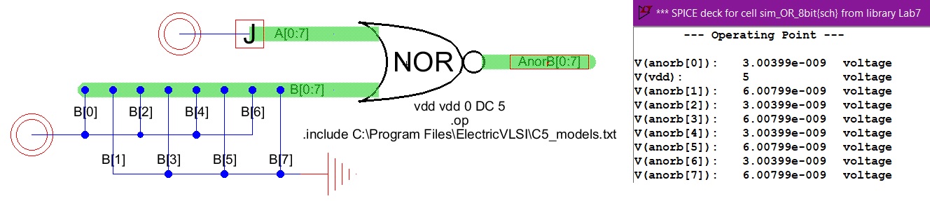
Figure 13. 8bit NOR gate simulation #1.
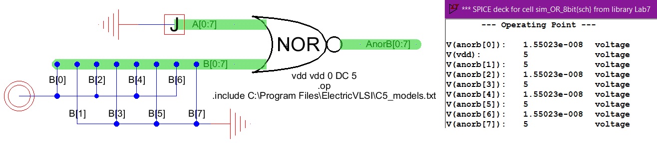
Figure 14. 8bit NOR gate simulation #2.
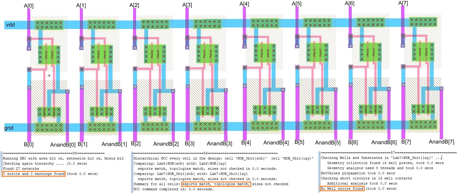
Figure 15. Finished 8bit NOR gate layout.
5. Discussion
For this lab, buses were introduced as a new method
in our ElectricVLSI training. I initially had a little trouble with the
simulation because it kept telling me that the wires weren't connected
to the bus via a bus pin. I tried all kinds of stuff and even ripped
the bus apart with the edit menu so I knew for sure that it used bus
pins but I still got the same DRC issue. It turns out I needed to label
the bus wire with the outputs (B[0:7]) before the schematic was able to
clear the DRC. I also assume that buses cannot be used in the layout
cell because the layout is a physical thing and buses are an "idea"
that is implemented to make a quick and efficient schematic. In
conclusion, the rest of the logic gates performed well and all the
layouts passed the DRC, NCC, and well check tests.