ENGR338 Lab Spring 2021
Lab 6: Build a NAND, NOR< XOR, and Full Adder
Name: Audra Benally
Email: albenally1@fortlewis.edu
1. Title: Build a NAND, NOR, XOR, and Full Adder
2. Introduction: In this 2 week lab, we built several logic gates
using pmos and nmos transistors. All the logic gates were simulated
using the C5_models.txt information. The last task hod us use all the
previously created gates to build a full adder.
3. Materials and Methods:
Materials:
- Computer
- LTSpice Software
- ElectricVLSI Software
- Pencil and Paper
Methods:
For this lab,
we built a NAND gate, a NOR gate, an XOR gate, and a full adder. All
the gates were built in schematic and layout view and were tested and
simulated. The results can be seen in the following figures. In the
last task, all the previously created logic gates were used to make a
full adder. The layouts were lengthened to the same height of about 122λ so that the full adder would be the same size. All the layouts were DRC clean, NCC clean, and had good well checks.
4. Results:
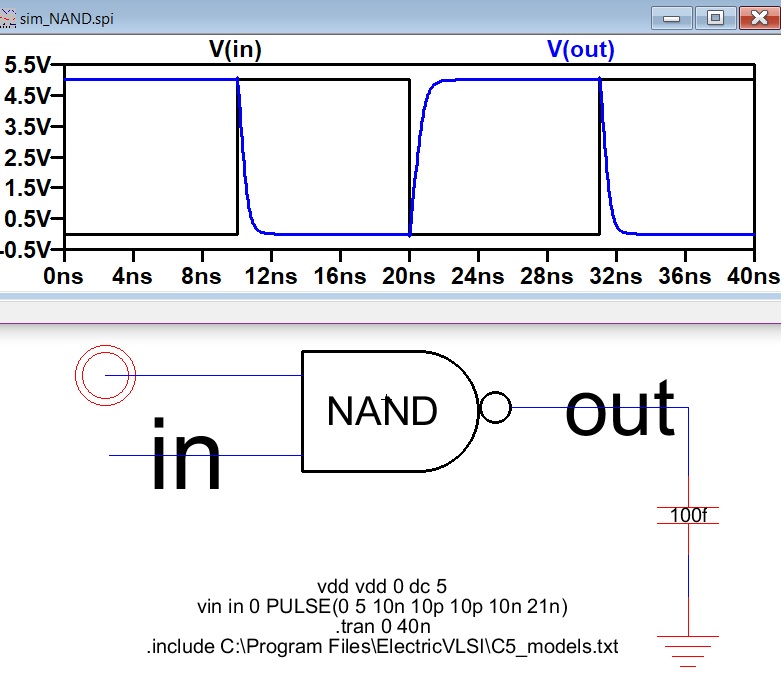
Figure 1. NAND LTSpice simulation.
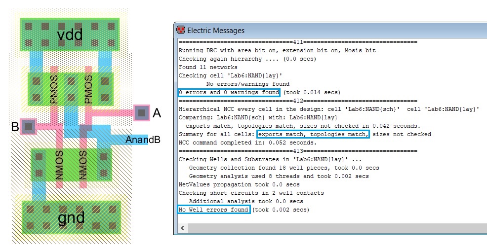
Figure 2. NAND layout with DRC, NCC, and well check results.
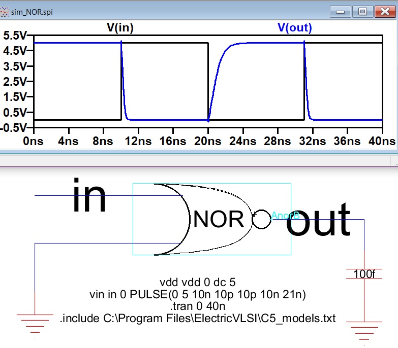
Figure 3. NOR LTSpice simulation.
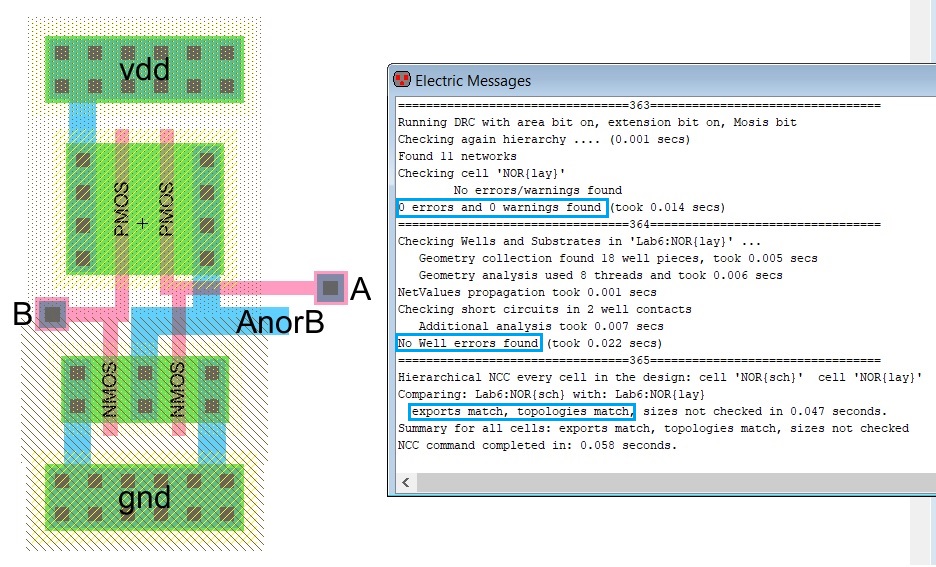
Figure 4. NOR layout with DRC, NCC, and well check results.
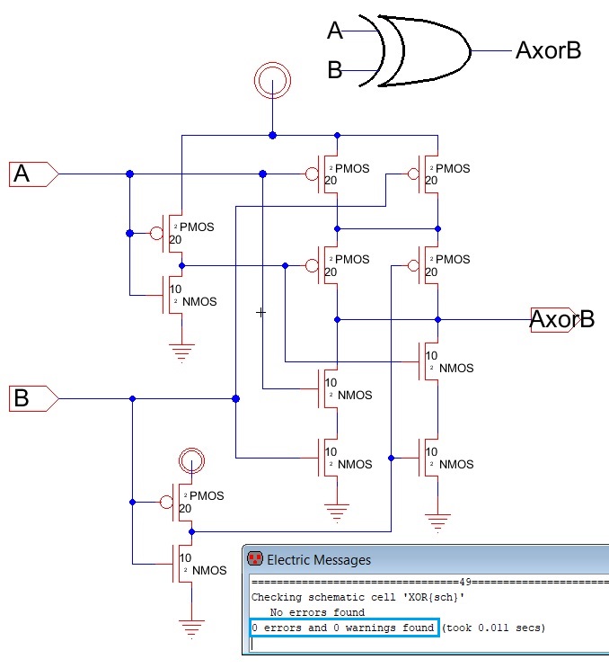
Figure 5. XOR schematic and icon with NCC results.
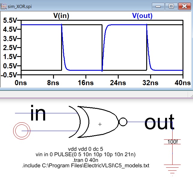
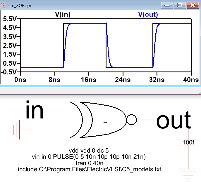
Figures 6 and 7. XOR LTSpice simulations.
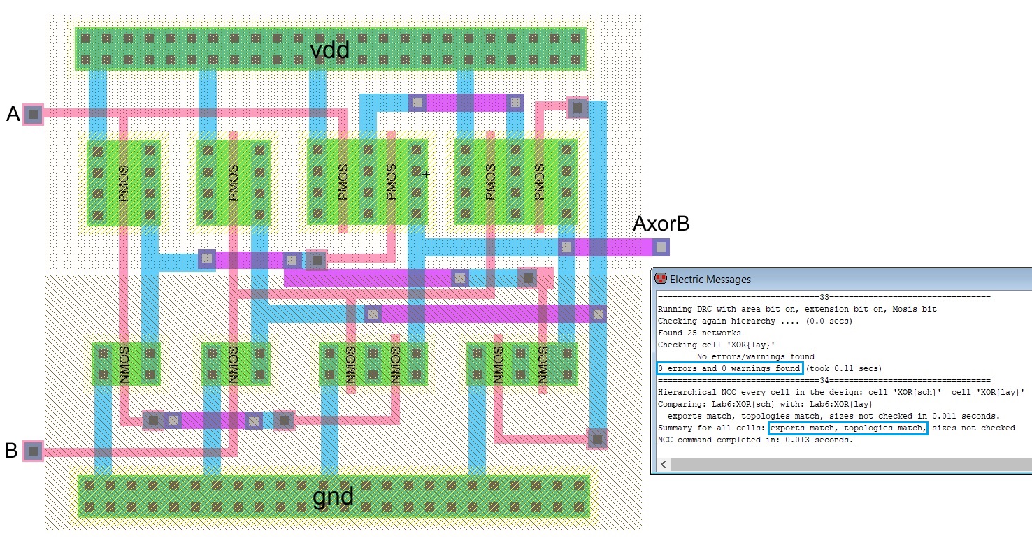
Figure 8. XOR layout with DRC and NCC results.
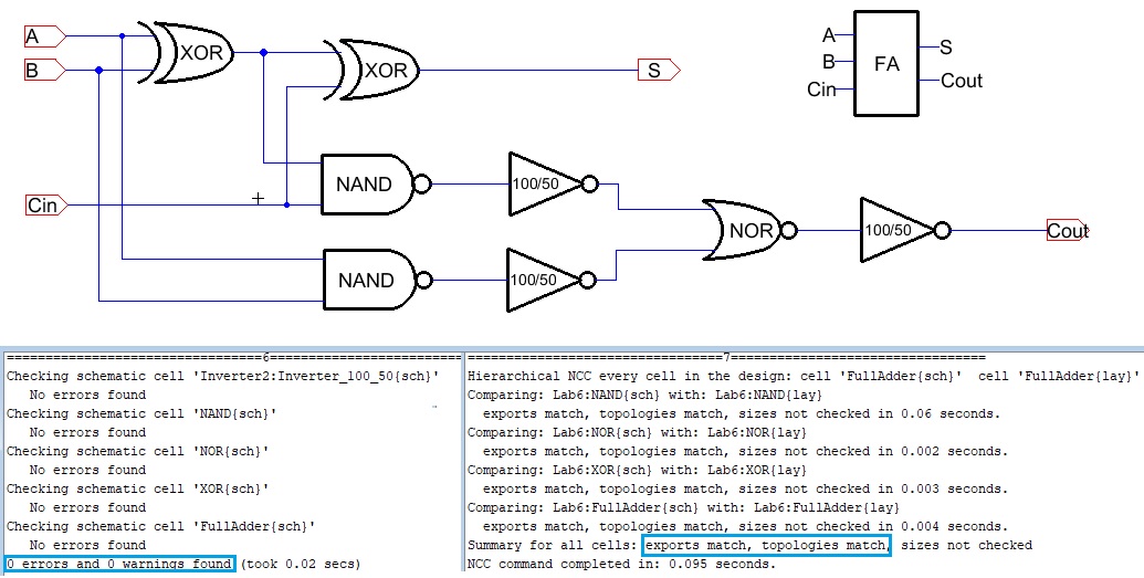
Figure 9. Full Adder schematic and icon.
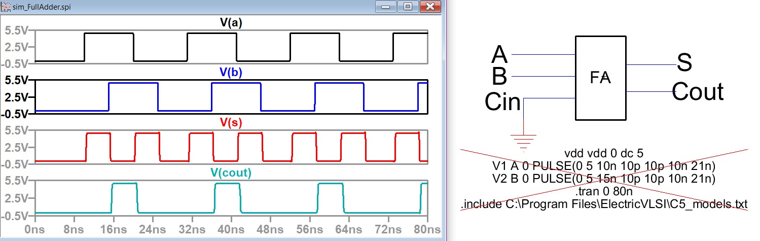
Figure 10. First simulation with the Full Adder. Cin = gnd = 0.
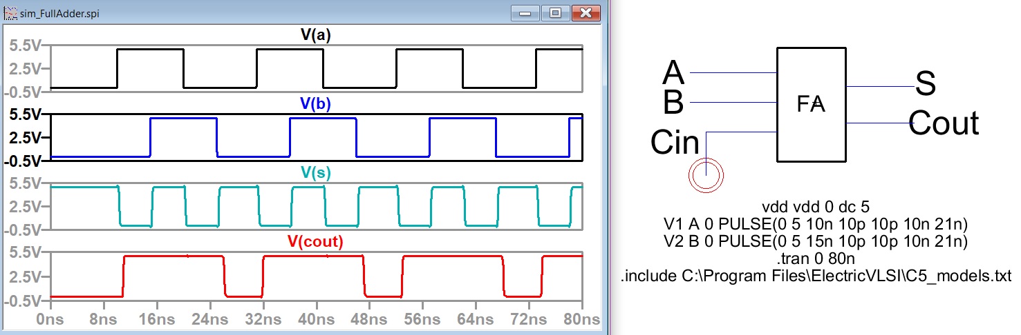
Figure 11.
Second sumulation with the Full Adder. Cin = vdd = 5V = 1.
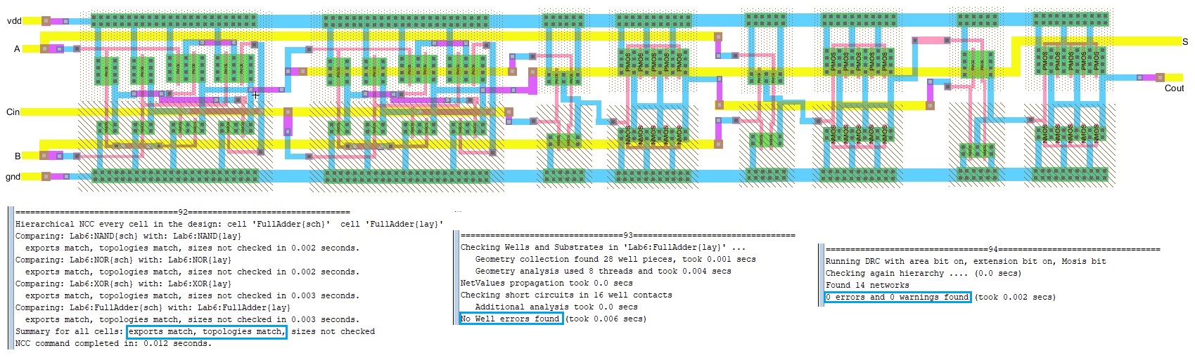
Figure 12. Full Adder layout with NCC, DRC, and well check results.
5. Discussion
This lab was super tedious and methodical so I had a
ton of fun. The only big problem I had was my NCC check not being clear
for the full adder. My topologies did not match and so I fixed it in
the schematic view. Other than that, all the tasks were manageable and
the lab ran smoothly.