ENGR338 Lab Spring 2021
Lab 5: The Inverter
Name: Audra Benally
Email: albenally1@fortlewis.edu
1. Title: The Inverter
2. Introduction: In this lab, we built an inverter in schematic and
layout view. This inverter had a PMOS with a width of 20 and an NMOS
with a width of 10. Next we used this first inverter to make a larger
inverter using the multiplier function in ElectricVLSI. The layout for
the larger inverter had a PMOS of width 100 and an NMOS of width 50.
The two inverters were connected to different sized capacitors and
simulated to test their driving capabilities. New built-in simulation tools were introduced in this lab as well.
3. Materials and Methods:
Materials:
- Computer
- LTSpice Software
- ElectricVLSI Software
Methods:
For this lab
we created two different versions of a PMOS/NMOS inverter. The first
inverter was a 20/10 inverter with 20/2 PMOS and 10/2 NMOS components.
The inverter was built in schematic view as seen in figure 1 first,
then in layout view which can be seen in figure 3. After schematic view
was made, code was added and simulated to show the simulation in figure
2. Then, a new inverter was made using the schematic of the first
inverter. A 5x multiplier was added through tools that turned the old
components into a 100/10 PMOS and a 50/10 NMOS. In the layout view the
PMOS and the NMOS were both duplicated and lengthened to what is now
shown in figure 5. Both inverters were simulated with three different
capacitors. The first had a capacitance of 100fF, the second was 1pF,
and the third was 10pF. The simulations for the first 20/10 inverter is
seen in figure 6 while the simulation for the 100/50 inverter can be
seen in figure 7. For the last task, different simulation tools were
used to test the two inverters. Figure 8 shows the ALS simulation tool
while figure 9 shows the same simulation with the IRSIM simulation tool.
4. Results:
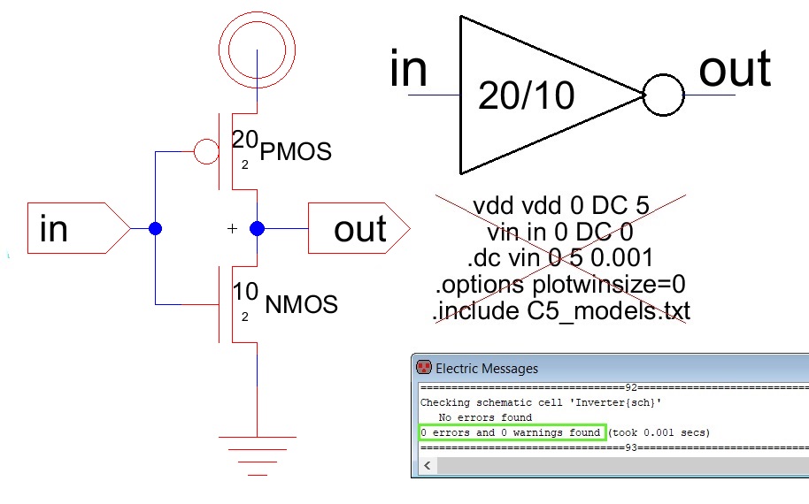
Figure 1. Inverter schematic for the first 20/10 inverter.
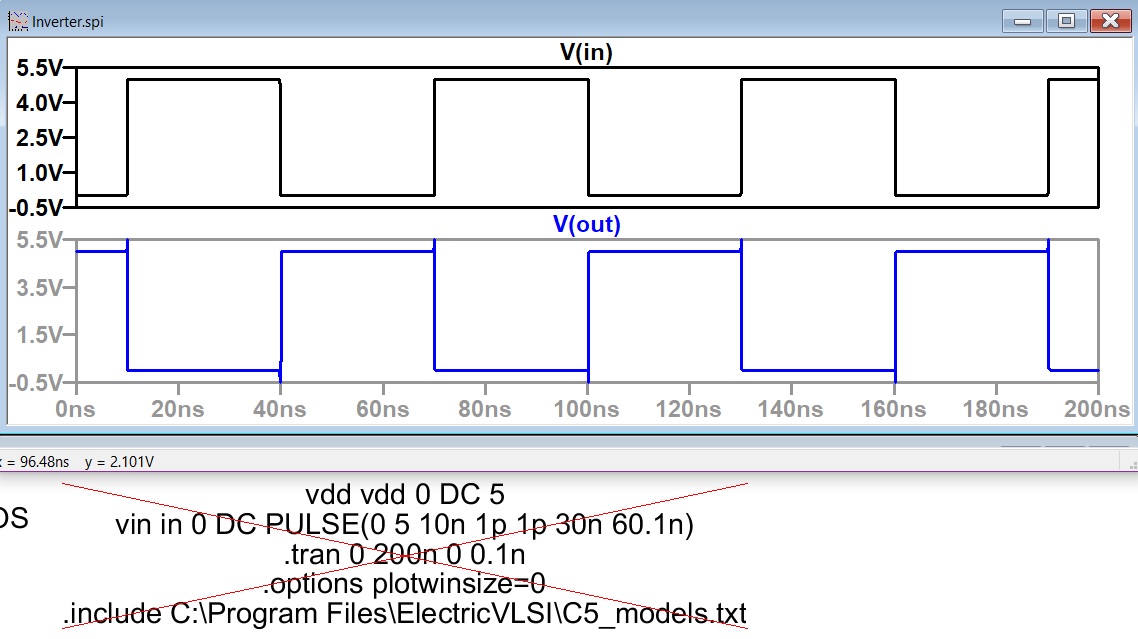
Figure 2.
Modified spice code to run a transient simulation using a PULSE()
Vinput.
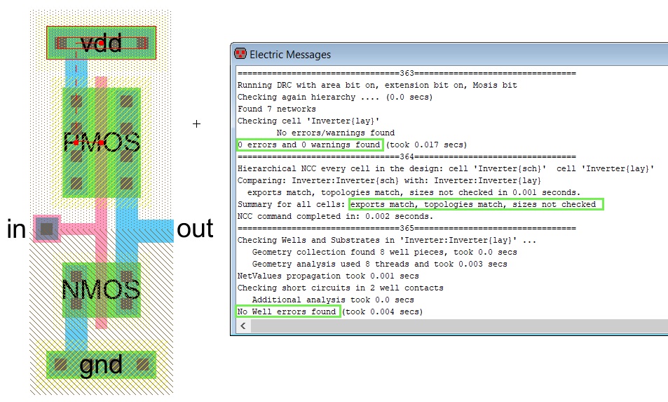
Figure 3.
20/10 Inverter layout with DRC, NCC, and well check results highlighted.
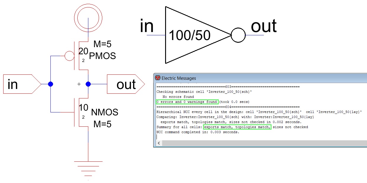
Figure 4.
100/50 Inverter schematic made from 20/10 schematic with M=5.
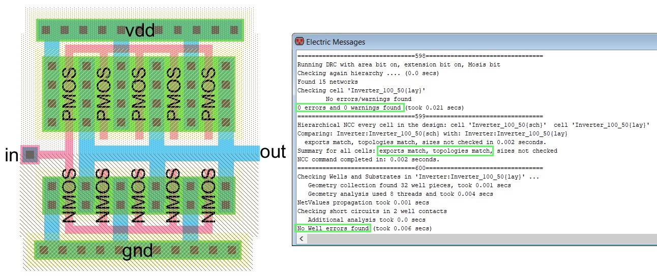
Figure 5.
100/50 Inverter layout with DRC, NCC, and well check results
highlighted.
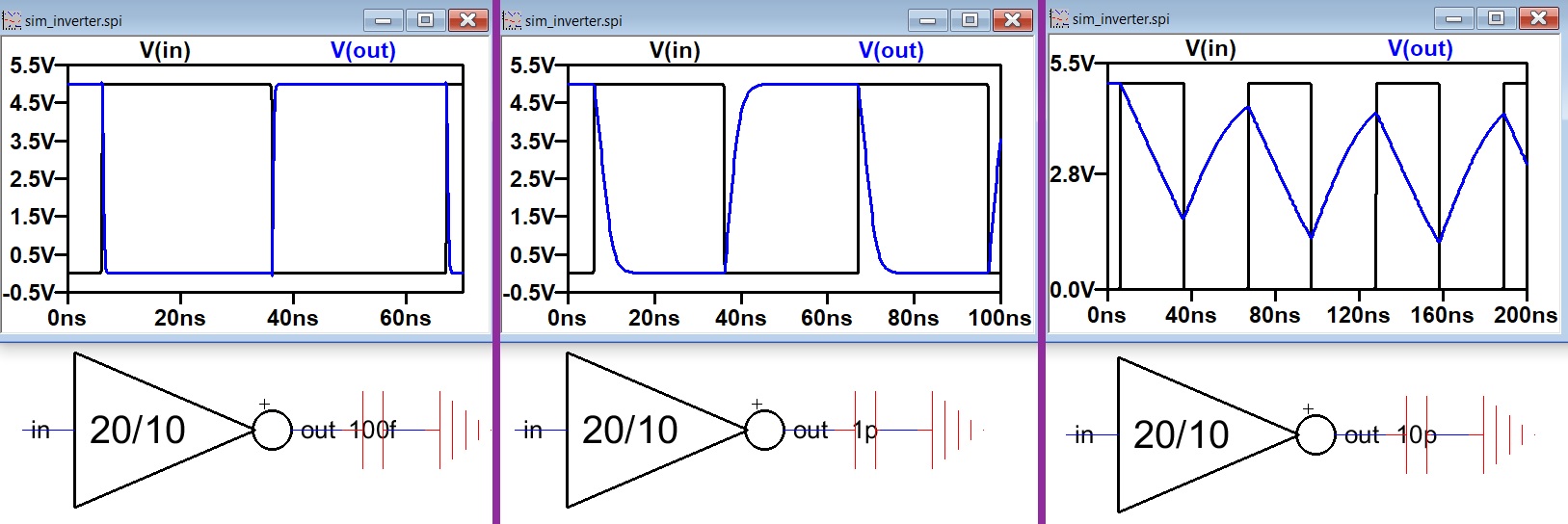
Figure 6.
20/10 Inverter with different capacitors and the resulting Vin/Vout
simulations. The simulations show the inverter's driving capabilities.
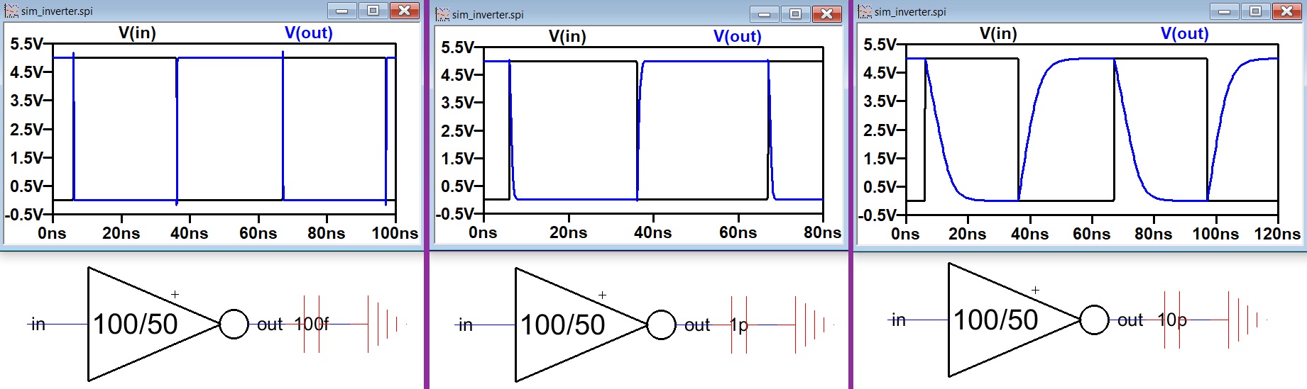
Figure 7.
100/50 Inverter connected to the same capacitors as the 20/10 inverter.
The resulting simulations are grouped with their schematics. The
simulations show the inverter's driving capabilities.
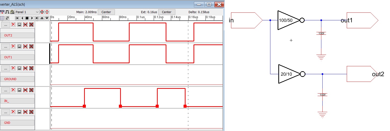
Figure 8. Simulation using the built-in ALS simulation tool.

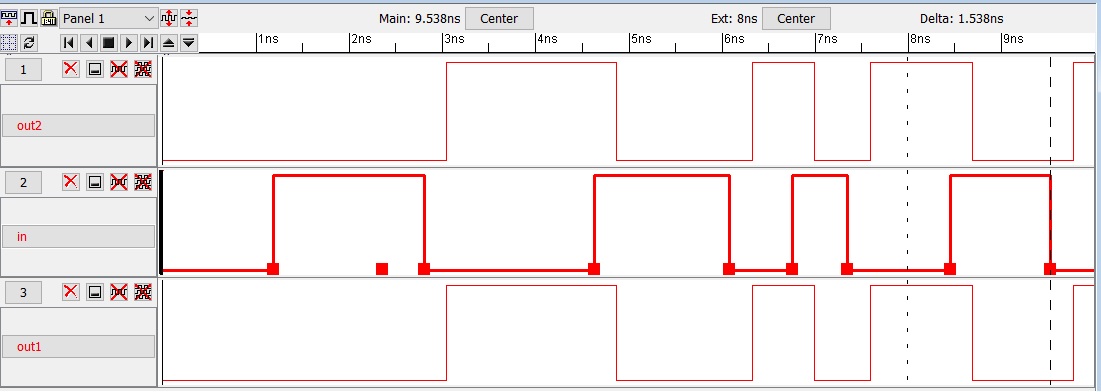
Figure 9. Simulation using IRSIM simulation tool.
5. Discussion
For this lab, two different
inverters were made. In the first task the schematic and icon were
created for the 20/10 inverter. The task also asked for a transient
simulation with a pulse input; the results can be seen in figure 2 with
the simulation on top and the code used below. In task 2 the layout was
made using single components of the PMOS pieces that were widened to
the 20/10 specs. The resulting inverter was DRC clean. NCC clean, and
had 0 well errors. In task 3, the spice tools multiplier was used to
add an M=5 multiplier to the duplicated schematic cell. For the layout
portion of the task, different components were duplicated and
rearranged into the inverter seen in figure 5. This larger inverter
layout also passed the DRC, NCC, and well checks. The fourth task had
several simulations to show the driving capabilities of both inverters.
You can see that there's a issue in figure 6 of the 20/10 inverter
where it is attached to the 10pF capacitor and the blue V(out) signal
is not fully reaching 5V or 0V. In the same situation you can see that
the 100/50 inverter is able to handle the 10pF capacitor without the
above issue. For the last task two new simulation tools were used to
test the circuit shown on the right side of figure 8. Both simulations
showed slight delay times of the outputs. No major errors were
encountered in this lab and much was learned about the potential range
and uses of inverters. Overall a success!!