ENGR338 Lab Spring 2021
Lab 4: MOSFETs and IV Curves
Name: Audra Benally
Email: albenally1@fortlewis.edu
1. Title: MOSFETs and IV Curves
2. Introduction: The purpose of this lab was to use the
ElectricVLSI sofware to build a PMOS and NMOS devices. The schematic
and layout were created for both MOSFETs. The finished products were
then simulated in LTSpice.
3. Materials and Methods:
Materials:
- Computer
- LTSpice Software
- ElectricVLSI Software
Methods:
For this lab
we created a PMOS and NMOS schematic and layout in ElectricVLSI. First
the NMOS was made using spice model "NMOS" and a 4-port transistor with
a width of 10λ, the outcome was similar but not quite the same as figure
1, yet. The PMOS was made in a similar fashion before DRC testing and
moving on. The NMOS layout was then created using an nMos node, 2 nAct
nodes, metal1, and a pWell node. The construction of the NMOS layout
can be seen in figure 2. The layout was DRC, NCC and well checked for
any errors before continuing. LTSpice code was added and the simulation
was ran with the layout. Once I knew the code worked properly, I moved
on the create the PMOS layout cell. The PMOS was made using a pMos
node, 2 pAct nodes, metal1-poly1 contact, and an nWell node. The fully
connected PMOS layout cell with the LTSpice code can be seen in figure
5. After the layouts were completely done and checked, the respective
codes were added to their schematics. Pins d, s, g, w, and ground were
all added and exported for the PMOS and NMOS schematics. Completely
finished schematics can be seen in figure 1 and figure 4. The IV curve
simulation results for the NMOS can be seen in Figure 3. The IV curve
simulation results for the PMOS can be seen in figure 6.
4. Results:
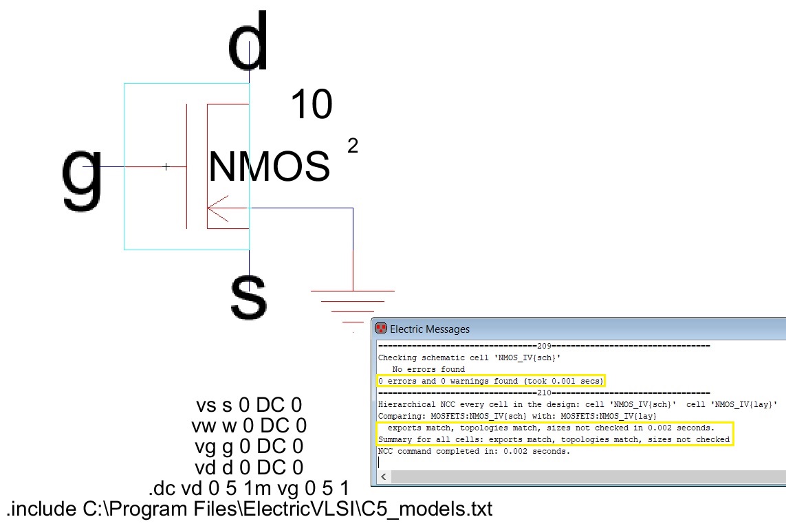
Figure 1.
NMOS schematic with LTSpice code. DRC is error-free and NCC matches.
The check results are highlighted.
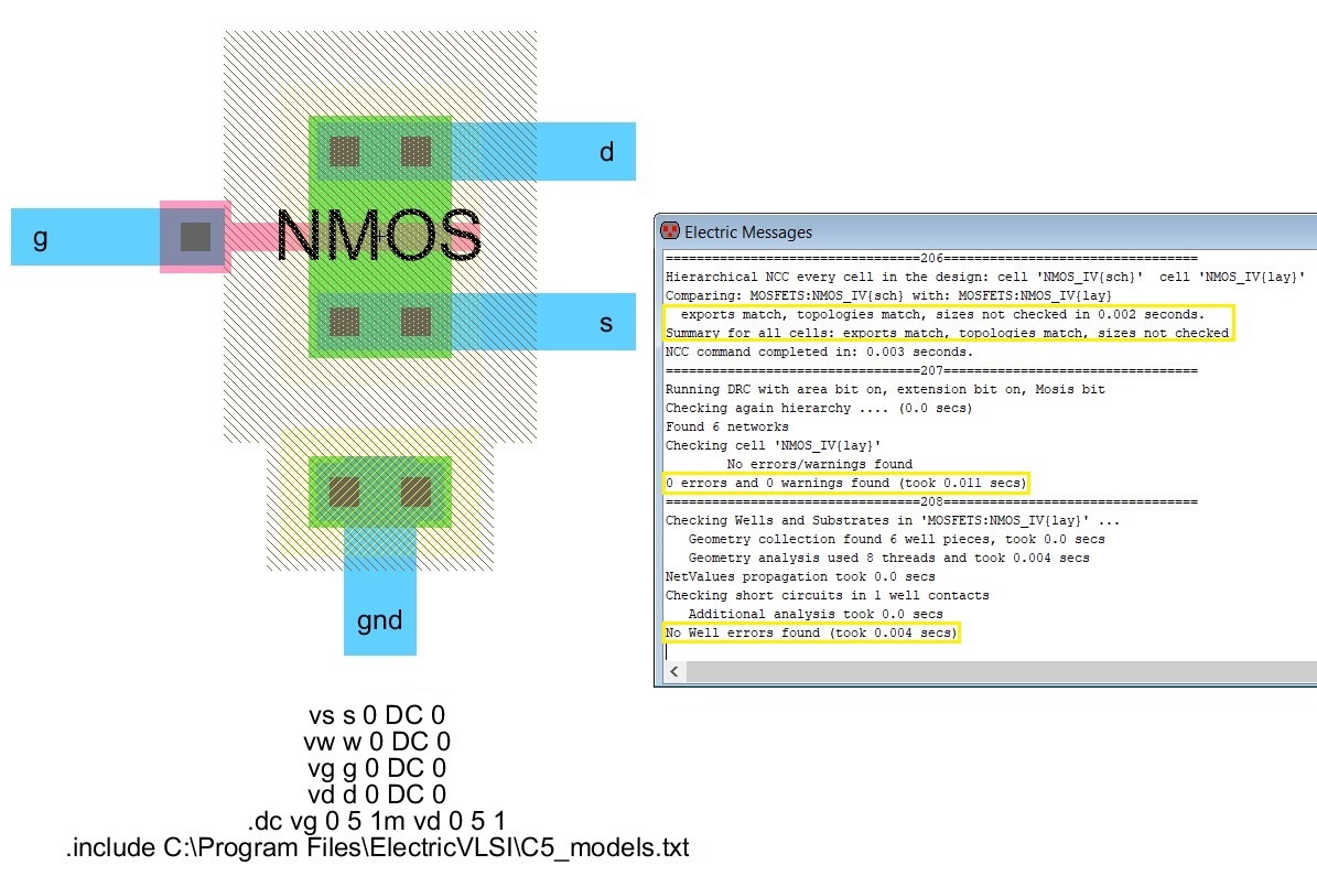
Figure 2.
NMOS layout with LTSpice code. DRC error free, NCC matches, and well
checks are error-free (highlighted).
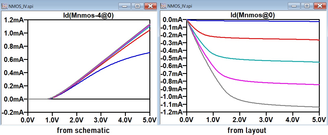
Figure 3. NMOS IV curves, the
left from the schematic with VGS increasing while different VDS values
filling the window. The right is from the layout with VDS increasing
and VGS steps filling the window.
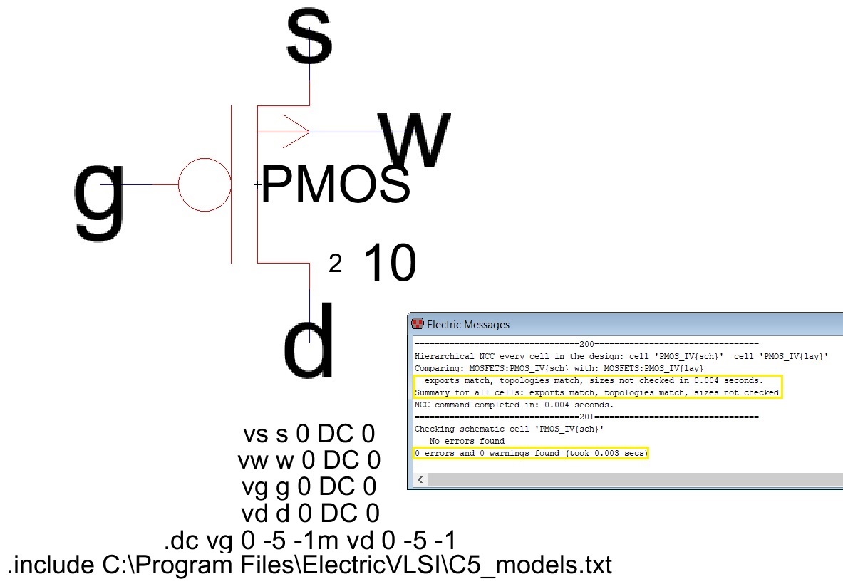
Figure 4. PMOS schematic with LTSpice code. DRC is error-free and NCC matches. The check results are highlighted.
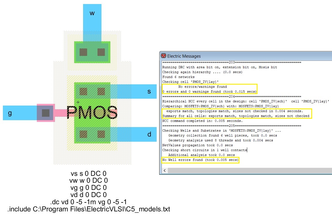
Figure 5. PMOS layout with LTSpice code. DRC error free, NCC matches, and well checks are error-free (highlighted).
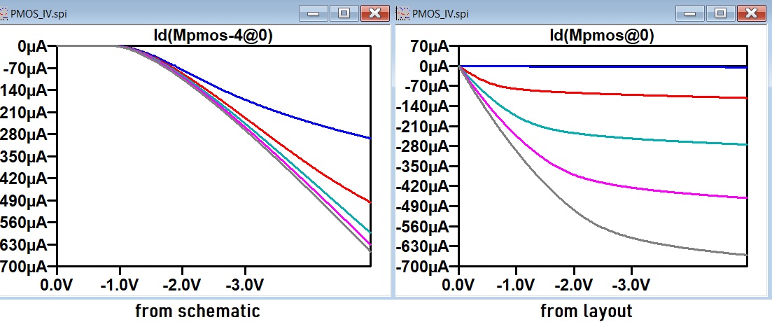
Figure 6. PMOS IV curves, the left from
the schematic with VGS increasing while different VDS steps filling
the window. The right is from the layout with VDS increasing and VGS
steps filling the window.
5. Discussion
For this lab, an NMOS and a
PMOS MOSFET was made in schematic and layout cells. The NMOS schematic
is made from a 4-port transistor so the layout and LTSpice code will
work. I followed all the directions except that during the simulation I
switched vg and vd in the schematic. I wanted to record both IDS vs.
VGS as well as IDS vs. VDS curves, and I also wanted to show
simulations from the schematic and the layout. I used the trace
Id(Mpmos-4@0)/Id(Mnmos-4@0) on all the simulations because I saw the
(Mpmos-4@0)/(Mnmos-4@0) selection on the tutorial and figured it was
the correct Id for the curves. Over half the simulations were upside
down but since voltages are relevant to where ground is considered I
thought it would be ok. I also wasn't sure if I should swich around the
traces that I was using. All of the cells were DRC tested and cleared,
NCC tested and cleared, and the layout cells passed their well checks
as seen in the yellow boxes in figures 1, 2, 4, and 5.