ENGR338 Lab Spring 2021
Lab 2: Design an R-2R DAC
Name: Audra Benally
Email: albenally1@fortlewis.edu
1. Title: Design an R-2R DAC
2. Introduction: The purpose of this lab is to familiarize
ourselves with the
ElectricVLSI software. We started by tweaking the software settings and
using given ADC-DAC schematic files to test the LTSpice simulation
settings. Next, we designed a R-2R ladder and replaced the ideal DAC
before simulating the circuit in LTSpice. Lastly, the R 2R Ladder B9
pin was isolated while a capacitor was connected at Vout. The resulting
simulation was used to find the time delay and compared to time delay
hand calculations.
3. Materials and Methods:
Materials:
- Computer
- LTSpice Software
- ElectricVLSI Software
- Calculator
Methods:
A large amount of the lab was
downloaded from the lab webpage. The first task was mostly to check if
the ElectricVLSI software was connected to LTSpice correctle so that
the schematic can be simulated in LTSpice. The resulting simulation can
be seen in figure 1. The second task was where an R 2R ladder was made
using 10k n-well resistors, pins, ground, and exported ports as seen in
figure 2. Once the icon was created for the R_2R ladder, the ladder
replaced the given ideal DAC and was run through an LTSpice simulation.
These results are shown in figure 3. In the last task, the B0 through
B8 pins were connected to ground while the B9 pin was left alone. A
10pF capacitor was connected to Vout and the simulation code was
changed to provide B9 with a pulse. The schematic was simulated to find
the time delay of the DAC. The resulting simulation can be seen in
figure 5 while the time delay hand calculations are shown in figure 4.
4. Results:
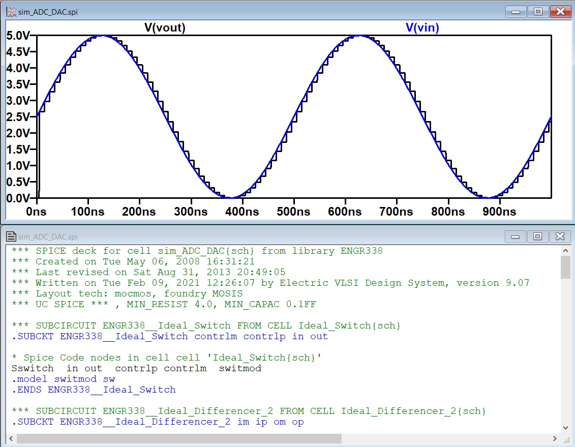
Figure 1. Output from the ACD-DAC given schematic.
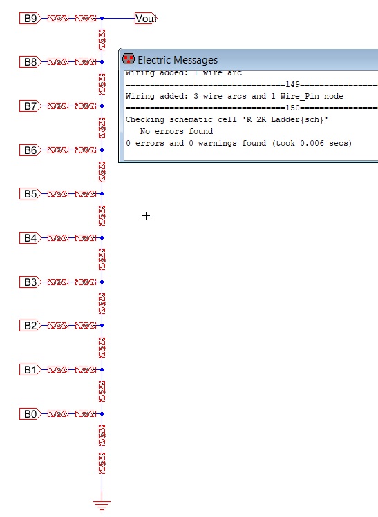
Figure 2. My DRC-clean R 2R ladder schematic.
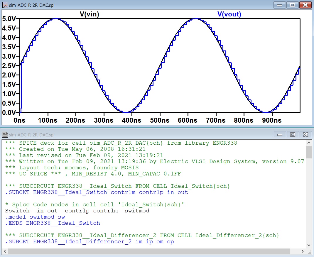
Figure 3. Output with the R_2R ladder in place of the given DAC.
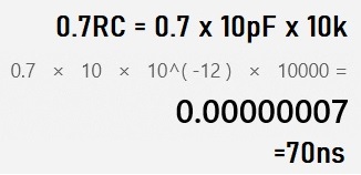
Figure 4. Time delay calculations.
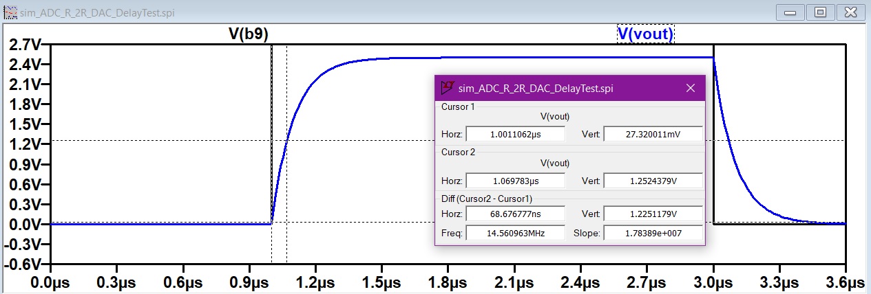
Figure 5.
Time delay simulation results. The time delay can be seen in the "Horz"
box under "Diff".
5. Discussion
In this lab, the ElectricVLSI
software was reviewed and used to make an R 2R Ladder DAC. I had
previously used the ElectricVLSI software on the school lab computers,
but this time I was able to set up the software on my own personal
laptop. It had taken a little while
to remember how to make the specific connections and export correctly
but after reading through the tutorials a little I was able to get
everthing done with very few issues.
All of my results were as expected. The R 2R Ladder was DRC-clean when
I finished it and had the same simulation results (Figure 3) as the
ideal given DAC (Figure 1). My DAC time delay in task 3 was a little
off but only by about 2 nanoseconds.