ENGR338 Lab Spring 2021
Final Project!!
Name: Audra Benally
Email: albenally1@fortlewis.edu
1. Title: Design an 8bit SAR Block
2. Introduction: For this class we had a project to build a SAR ADC
in LTSpice. After a couple weeks though the entire SAR ADC wasn't
feasible so the project was changed to creating and simulating just the
SAR block. The SAR block was made using sub-designs for each level with
testing via simulation before moving on to the next level. First a 3
input NAND gate was made (figure 1) and simulated (figure 2), then the
gate was used to build a TI DFF (figure 3). After the TI DFF was tested
for any
bugs (figure 4), it was used to make the 8bit SAR Block (figure 5). The
simulation results for the SAR block can be seen in figure 6.
3. Materials and Methods:
Materials:
- LTSpice Software
- Computer
- Computer Mouse
Methods:
The
first thing that was made in this project was the 3 input NAND gate. I
had an old NAND gate already created so I added another input and
edited the symbol. I got the short channel lengths from Dr. Baker's
CMOS book via Homework 3. For the simulation I staggered some pulse
inputs for A, B, and C to get a variety of inputs to check. The
simulation appeared correct so I moved on to the TI DFF. The layout was
copied from the version on the yilectronics.com website. The TI DFF
layout worked well in the simulation and so the icon simulation ran
smoothly with no issues. The SAR block was next. We were provided with
a 4 bit SAR block layout and simulation on the project site to
reference for our 8 bit SAR block. Since it's 8 bit the SAR needs 9 TI
DFFs. The SAR block had a little more issue when I changed out all the
simulation components for icon pins but it was a quick fix. The final
simulation was successful.
4. Results:
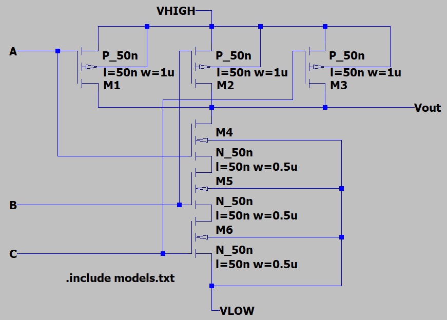
Figure 1. 3 input NAND gate at the PMOS level.
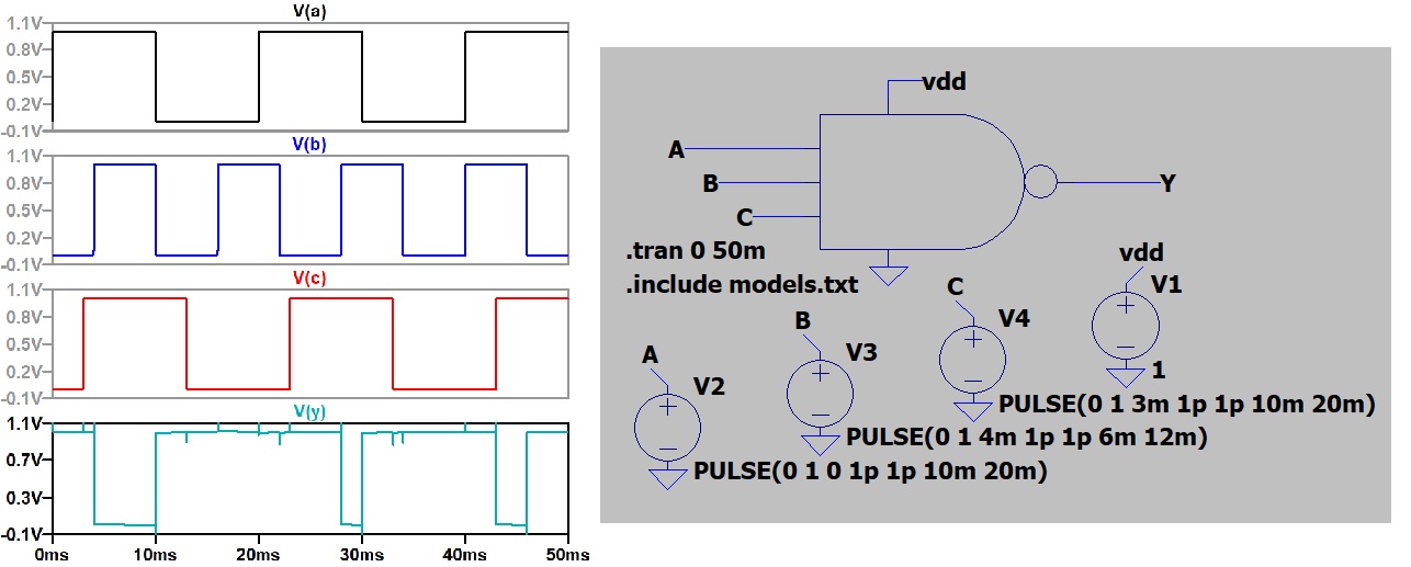
Figure 2. NAND gate simulation.
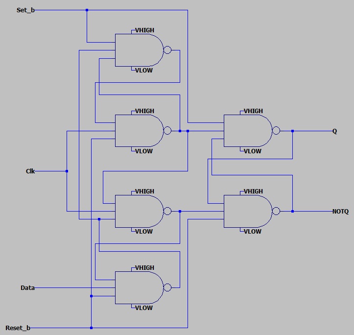
Figure 3. TI DFF made from the 3 input NAND gate in figure 1.
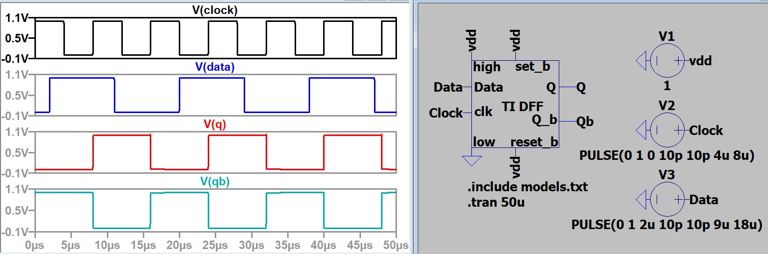
Figure 4. TI DFF simulation.
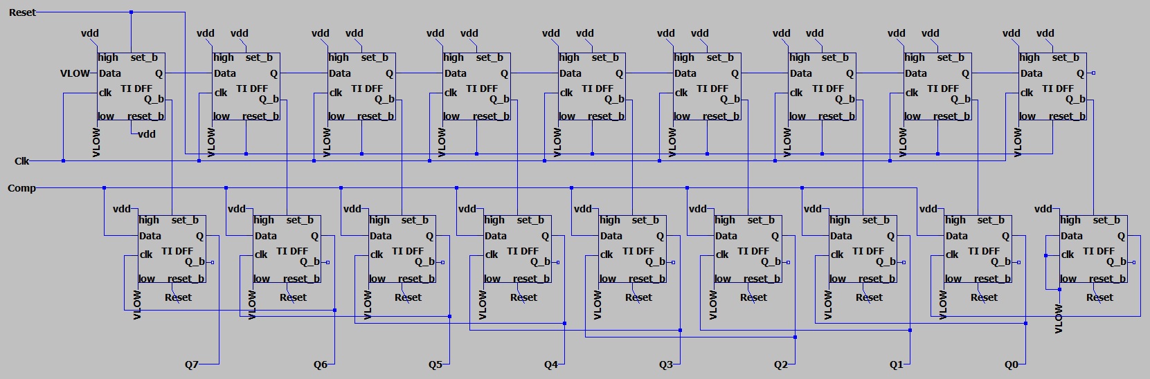
Figure 5. SAR Block layout using the TI DFF from figure 3.
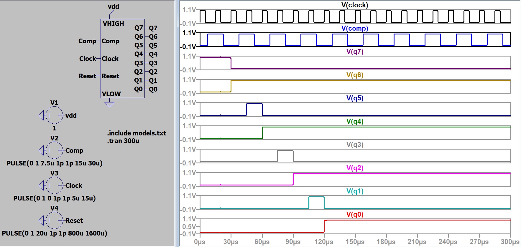
Figure 6. SAR Block simulation results.
5. Discussion
This project was a nice change of pace from working on ElectricVLSI all
semester. I had a little trouble in the beginning with the NAND gate
because I forgot to change my lengths and widths of the PMOS and NMOS
parts in the NAND gate layout. Once I realized what was wrong my
simulation for the NAND gate worked correctly. Building the TI DFF ran
smoothly and the only hiccup I had during the simulation was forgetting
to change the set and reset inputs from Gnd to Vdd because I had
originally put inverters in the TI DFF but changed it to match the
project guidelines online. The
SAR block design came together well and was fun with all the wires
everywhere. I ran the first simulation in the layout before converting
it to a more icon-friendly version (vlow instead of gnd, etc..). While
I was putting in vlow pins I had forgotten to put a vlow pin on the
Data pin on the first TI DFF. I didn't realize until I simulated the
SAR block again with the icon and all the outputs were 1. After a good
thorough check I realized my error and fixed the issue. After this one
problem the simulation ran correctly. I really enjoyed making these
circuits in LTSpice and I wish I had known about this free software
when I was first starting out in my Engineering path. I really enjoyed
circuits (one of the reasons I went into computer engineering) but I
went to a community college so I didn't really get to build or simulate
anything. This was super fun and I greatly enjoyed building and testing
this project.