CE338
Digital VLSI Design Course Project - An 8-bit SAR ADC
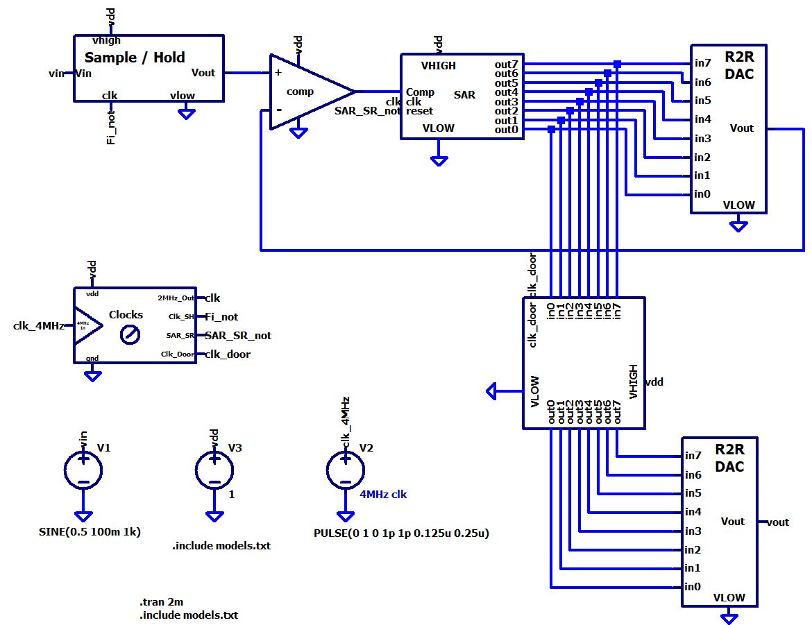
1. System
overview
This SAR ADC uses the 50 nm
technology from Dr. Baker's CMOS textbook. The entire LTSpice folder
(in the 50nm technology) which includes the
model file can be downloaded here. This could be used as a reference.
The system diagram is shown
below.
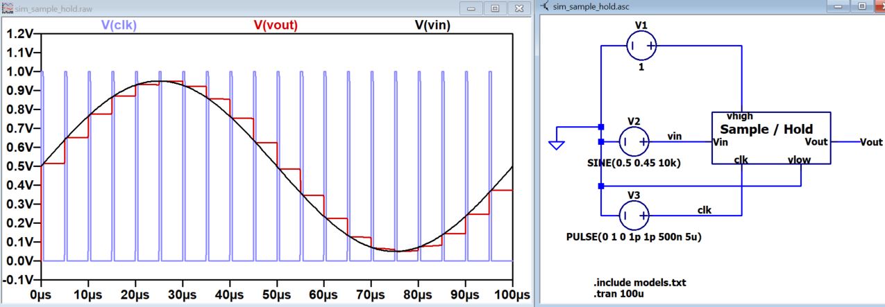
2. The
sample and hold circuit
The sample and hold circuit
was published by Abo et al in 1999 (Abo's
1999 paper)

Please note that it is ok to
use 50% duty cycle clock to run the
sample and hold circuit. However, the AD conversion only happens during
the 'holding' period, so the sample/track time only needs to be just
adequate to acquire the analog value and then give the rest of time to
the
'holding' state. In the following simulation you can tell that the duty
cycle is < 20%.
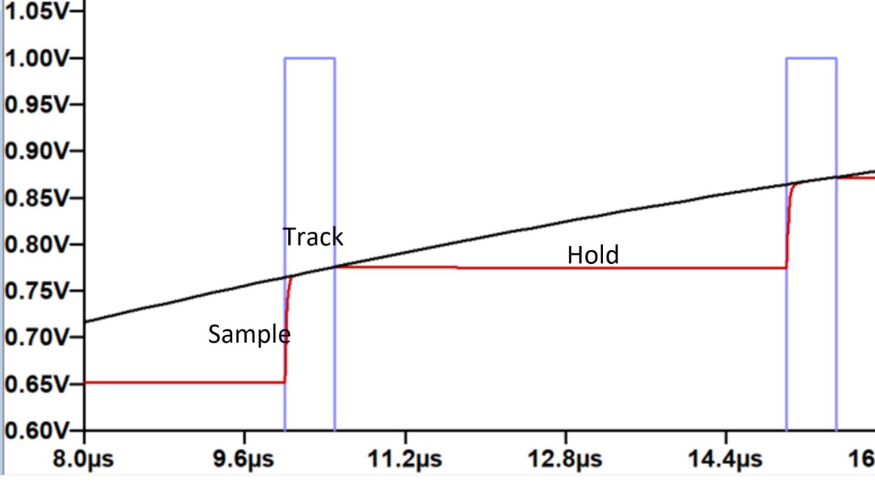
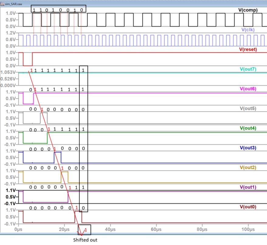
During the 'holding' period,
the 8-bit SAR ADC runs the data conversion
which requires 10 rising edges. 9 for the 9 states to complete the SAR
algorithm, the last is to send the data out.
If you probe VG, you will find that VG is tracking the input signal:

3. The
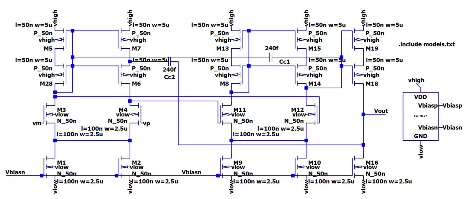
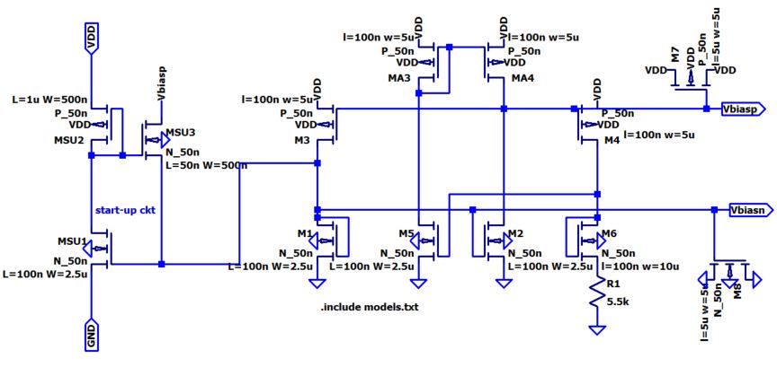
operational amplifier
The op amp circuit came from
Dr. Baker's textbook (Figure
24.61). Please note that the biasing circuit is usually not shown in
the op amp's circuit. The
following op amp is not good at lower volages that are close to 0 V.
From the following transient analysis of the final design of the ADC
you can find that lower voltages have poor accuracies.
A rail-to-rail comparator is recommended
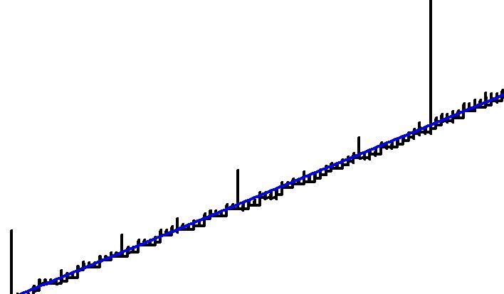
The following simulation can be used to find out DNLs and INLs. However, the performance at lower voltages are pretty poor.
Please
note that you won't be able to run a DC sweep to get this curve since
the ADC needs to be clocked in the time domain. In the following
simulation, I used transient analysis with a slow rising edge of
a pulse and I only simulated the rising edge part of the pulse.

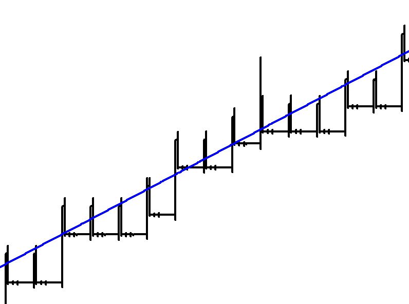
Zoomed in view :
The simulation SPICE code can be found in the following figure.

The schematic of the biasing
circuit
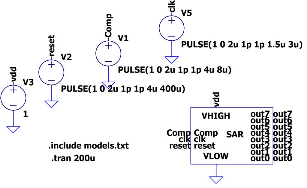
4. The SAR
block
No magic here. As a pure
digital circuit, it just operates as expected.

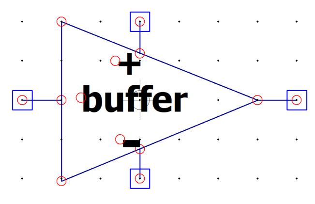
The triangle shape parts are
buffers which strengthens the driving
capability of the clock. It may not be very necessary for the
simulation but it helps the real circuit since there are many stages in
which every stage contributes a capacitive load.

(Figure credit: Audra Benally)
In your report, you must show
the simulation results of the SAR block to demonstrate that it
implements the SAR algorithm.
5. The
R-2R ladder DAC
In this project, you need to
use the same DAC twice. One is used
inside the SAR ADC system, the other one is used to conver the overall
digital output into an analog signal so you can probe it and show it in
one single plot pane in LTSpice.
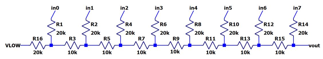
(Figure credit: Audra Benally)
6. The
timing block and the 'door' register
Understand and implement the
timing of the SAR ADC takes 80% of the
effort in the overall design. You must know what the circuit does at
which time period to design the circuit. The
inverters connects to Q1 - Q4 of the counter have smaller ratio (2/1
PMOS/NMOS) which avoides some kick-back surges from large gates.
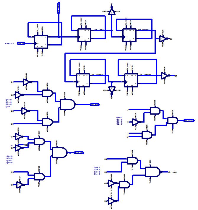
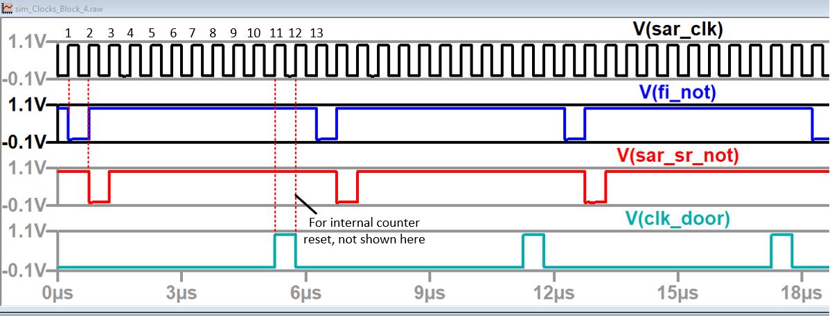
Notes that explained the timing and S/H.
The TI DFF holds the previous
values when clk is 0.

The 'door' register is very
simple:

7. Results
I simulated my circuit and
shows the following result (it took me over 1 hour to complete this
simulation on a core i7 HP Zbook)

Zoom-in view:

---------------------------------------
Course
project tasks: (100
points)
1. Use the C5 technology and build this ADC in ElectricVLSI. You must use C5 which means the
VDD will be 5 V not 1 V. You must include simulation
results and discussions of each function
block to receive credits, and of course, it must be DRC/NCC clean. (85
points)
We may be able to build it in Cadence Virtuoso using TSMC 180 nm PDK. Let's see if things will be ready after the spring break.
2. Design your SPICE code and experiment to plot and measure DNLs and INLs of the ADC. (15 points)
Refereces:
The
columbia VLSI desgin lab
Abo's
1999 paper.
Audra
Benally's summer 2021 report
UAE
Master's Thesis
Razavi
Bootstrap Switch
Old
SAR ADC flies
The CMOSedu opamp.zip