CE338 Digital VLSI
Laboratory
The Inverter
Objectives:
Be able to layout and simulate an inverter in Electric.
Lab Tasks:
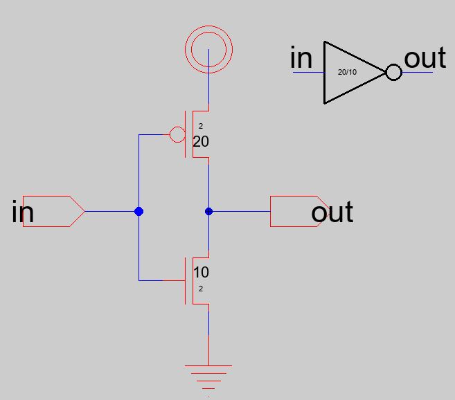
** Task 1: Create the
schematic of the inverter.
Note that
the bigger size of the number denotes the 'drain' side. Please a PMOS
and an NMOS in the schematic view, rotate/mirror the PMOS to let the
drain oriented to the NMOS. The PMOS is 20/2, the NMOS is 10/2.

Use
the vdd and gnd symbols (they are global
exports by default so don't export them again). Export the 'in' and
'out' ports for the inverter. Build create an icon view of it.
Run
the DRC check to ensure it is error free.

Next,
run a simulation to ensure that it inverts
the input. Do not forget to set Spice models by selecting the PMOS or
the NMOS one at a time and follow Tools - Simulation (Spice) - Set
Spice Model. Name them as PMOS and NMOS respectively.

Next,
run a transient simulation use a PULSE()
input. The spice code is not provided here. Design it one your own.
The results looks like this:

** Task 2: Create the
layout of the inverter.
Build the
layout of the inverter by following the tutorial
here.
Run DRC and LVS
check before you move forward. Also, do not forget to set the Spice
models for the PMOS and the NMOS.

** Task 3: Use the multiplier to build a larger inverter.
The inverter you
just built is 20/5
and 10/5. In this section, let's built a 100/2 and 50/2 inverter using
the multiplier function in Electric.
First, duplicate the inverter cell and rename it as
'Inverter_100_50'. Click the new cell and select the PMOS. Then press
tools --> Simulation (spice) --> add Multiplier to set
the M=5
adding 5 parallel PMOS. Do the same to NMOS. Others are kept the same
as before. We can get the following circuit.

In the layout view, copy/paste the existing PMOS, delete the metal
contacts on the left side of the duplicate, then make the connection to
the left. Make sure that the connection is built by the green wire (the
active field) not the metal (blue).

After you done with the first duplicate, run a DRC check instantly
before you moving forward. The gap size indicated in the following
figure must be evenly spaced.

Get 5 of the PMOS and the NMOS in parallel and make them 5 times wider.
Run DRC/LVS after this is done.

** Task 4: Run simulations to verify the driving capability of these
two different inverters.
First, create a simulation schematic view for the 20/10 inverter:

Run 3 simulations to let it drive 100 fF, 1 pF, and 10 pF caps
respectively.
Cload = 100 fF

Cload = 1 pF (start having some difficulties to drive the cap).

Cload = 10 pF (can't drive it to the full voltage).

Next, let's grab the wider inverter and see how it goes. (you can
directly replace the 20/10 one with the 100/50 one).
Cload = 100 fF

Cload = 1 pF

Cload = 10 pF
Now, you can tell the difference. The 100/50 inverter can drive bigger
caps compare to the smaller one.

Lab reports
grading
rubric:
Task 1: 25
points.
Task 2: 25
points.
Task 3: 25
points.
Task 4: 25
points.
-------------------------------------
The end of the lab.