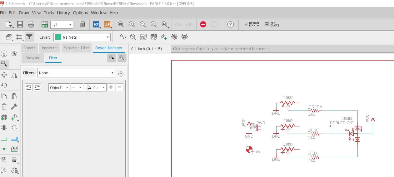
Save the LED schematic to your project folder. Double click to open up the schematic in Eagle.
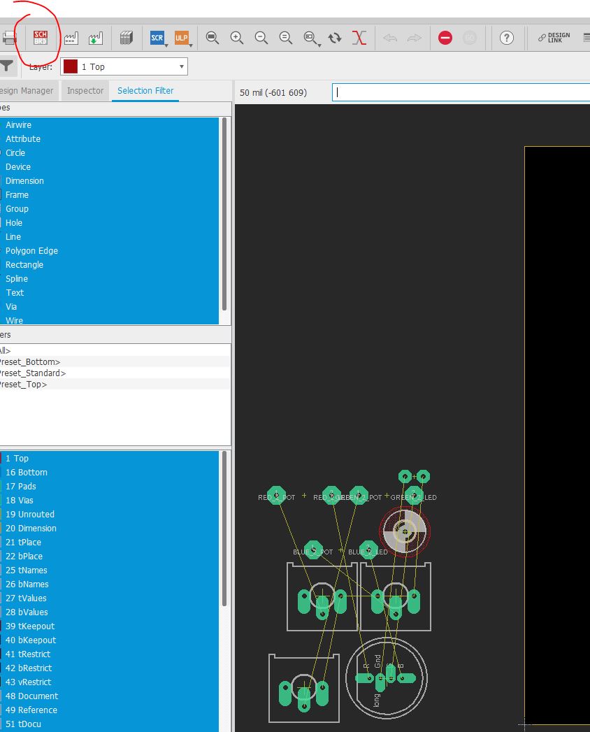
Press the following button to switch to the layout view.
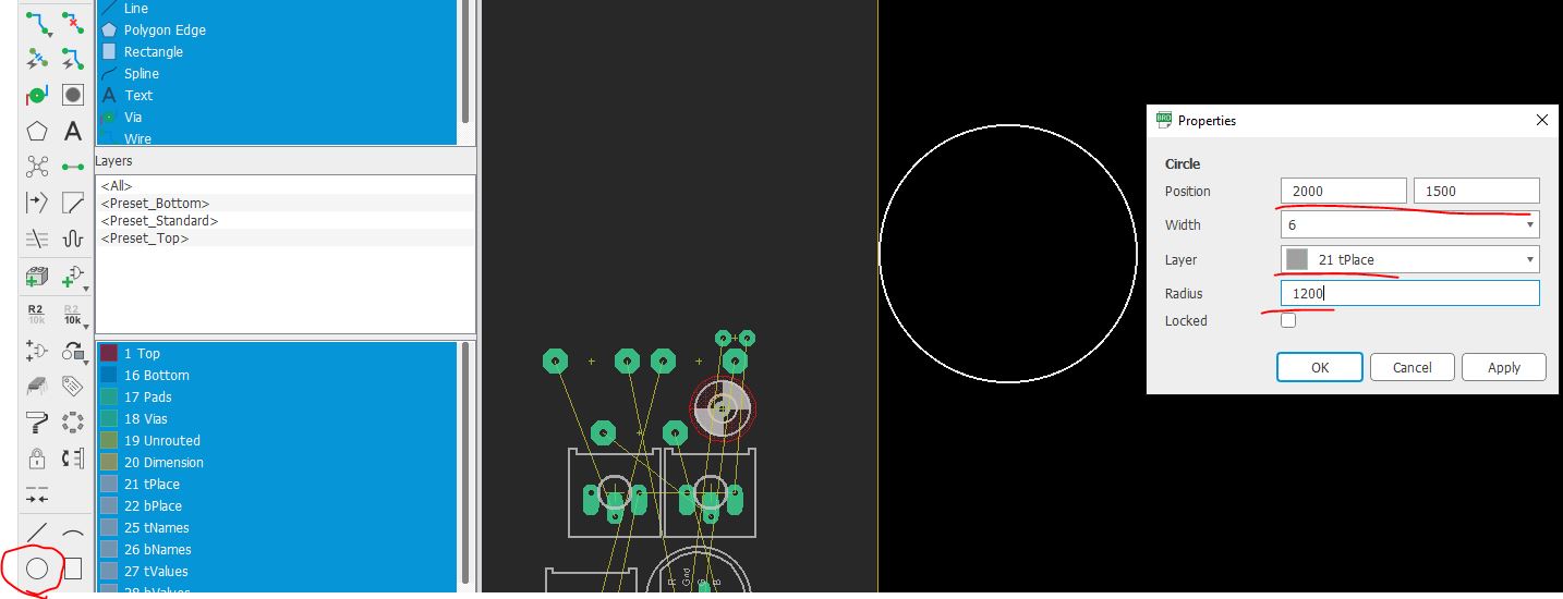
Select the circle tool and draw a circle at the tPlace layer.
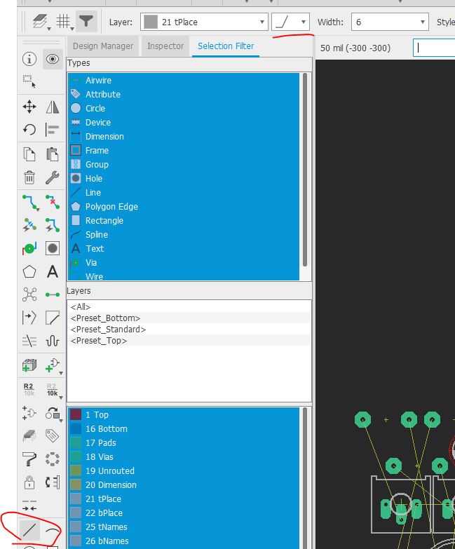
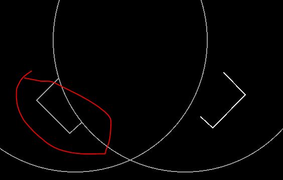
Use the line tool, to draw the fins. Make sure that you select the tPlace layer and the Bend Style 2. Width is 6.
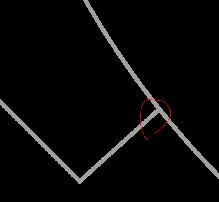
Draw one on the left hand side first. Zoom in to make sure it joins the circle outline.
Draw
one then select it - copy it - drag to a different place and hold the
left mouse button then press the scroll wheel of the mouse to mirror
it.
To
draw the dimension layer, you must close the outline in order to create
a valid dimension of the PCB. Please watch the demo video to make sure
you do it right.
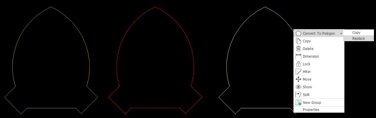
Copy/paste the shape drawn in the dimension layer twice.
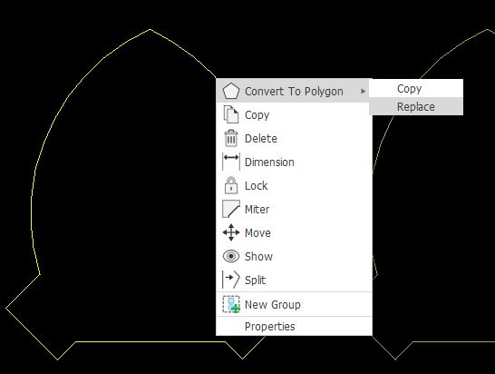
Start with the second one, right click and convert it to polygon with the 'replace' option.
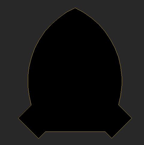
It changes to the following view.
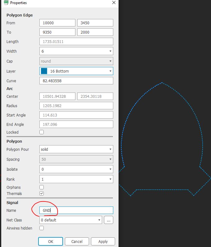
Then right click the edge of the shape, choose perperties. Switch it to Top, change width to 6.
Move to the third one.
Change it to the bottom layer.
Connect top polygon to VCC and bottom polygon to GND.
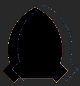
Move the outlines drawn in Dimension, Top, and Bottom to one (overlap them).
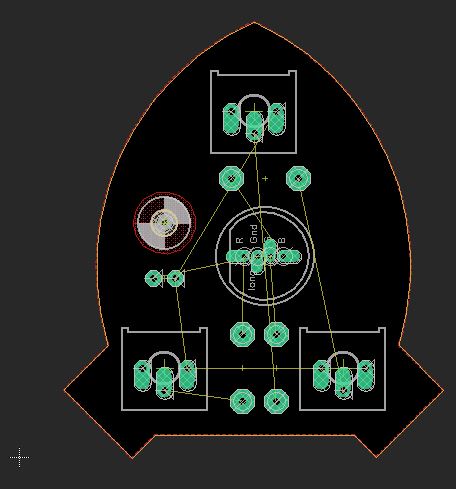
Put the components into the shape. If you haven't created the schematic yet, create it.
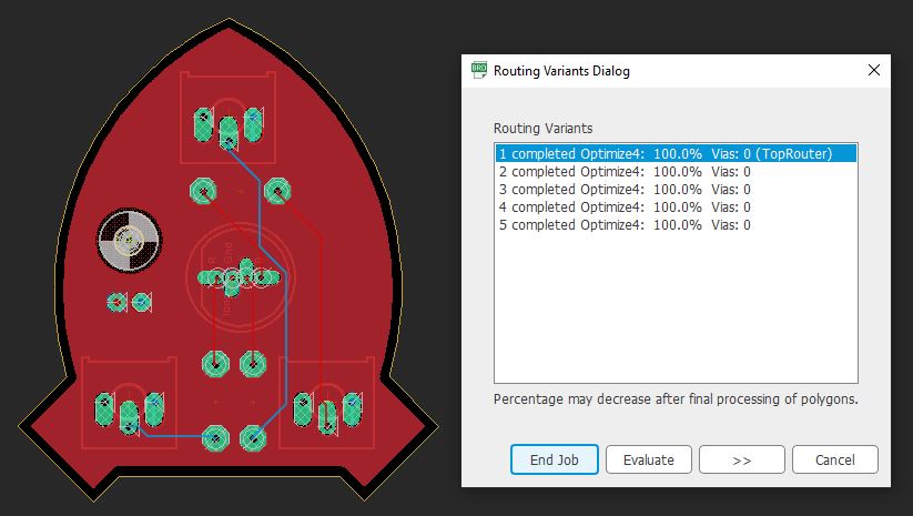
Do a quick routing job to see if it works. If you are required to hand-draw it, you could ripup things and re-draw it.
Check a set of VCC or GND through holes to see if they are connected.
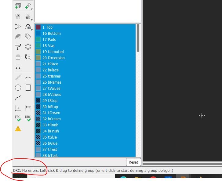
Make sure it is DRC clean.
Follow
Dr. Coulston's Lab03 instruction and use the following demo as a
reference to design your rocket shape of the PCB outline.
(Sorry for the bad resolution, I lost the video that has a better resolution)