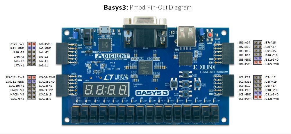
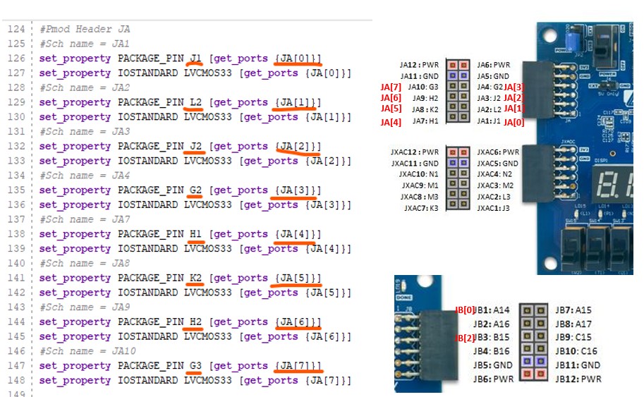
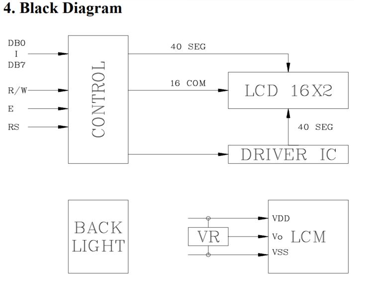
JA[0:7] is connected to D0-D7 JB[0] is connected to EN JB[2] is connected to RS FPGA GND to breadboard GND Elegoo module plugged onto a breadboard VO to potentiometer's output, potentiometer's two terminals are GND and 5V respectively Backlight - A to 3.3V, K to GND LCD VDD to 5V, VSS to GND
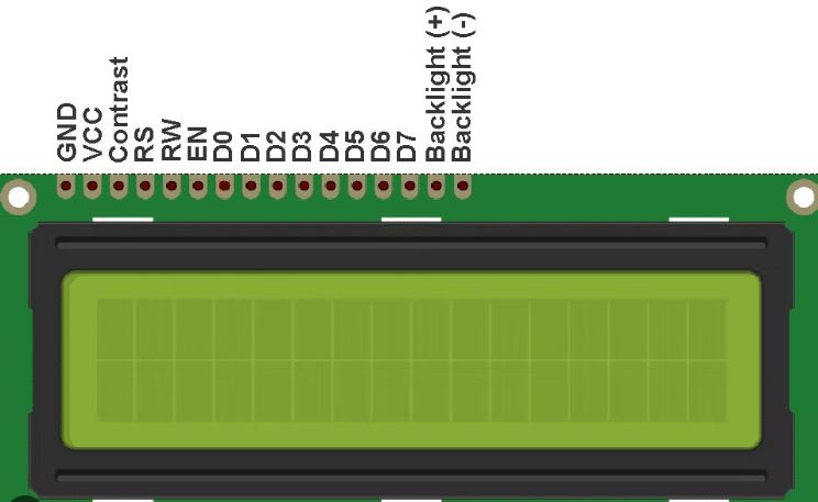
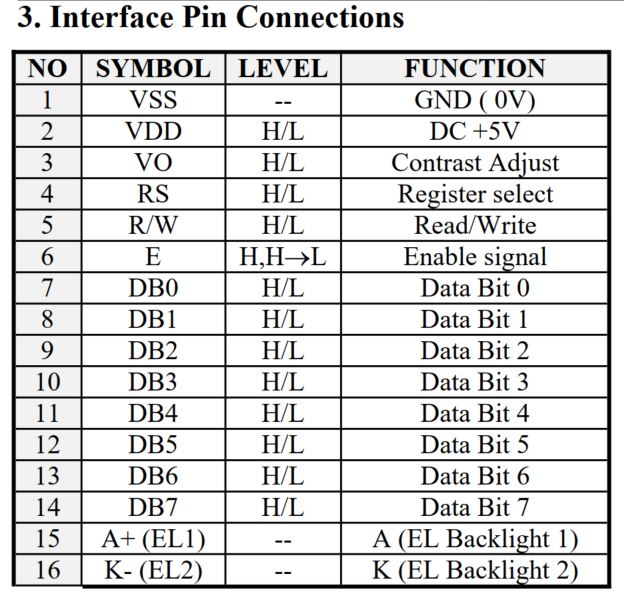
GND = VSS, VCC =
VDD, Contrast = VO, E = EN
The
GND (VSS) and VCC (VDD, +5 V) pins are the power supply pins. The VO
pin is used to adjust the display contrast. We can use a potentiometer
to connect VO to a suitable positive voltage below +5 V. The Led+ (A)
and Led- (K) pins are used to turn on the display backlight, connect K to GND, A to 3.3V from the Elegoo power module.
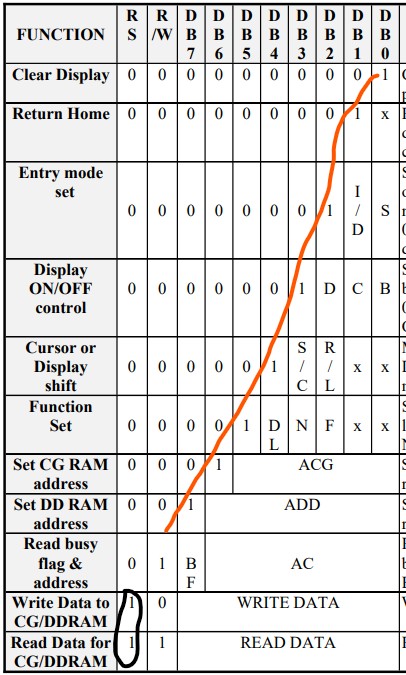
The
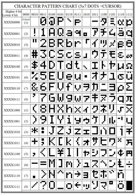
RS pin is the Register Selector pin for the LCD controller. The HD44780
has two registers: an Instruction Register (IR) and a Data Register
(DR). The RS pin is a control pin that specifies whether the IR or DR
should be connected to the Data Bus (DB0 to DB7 pins). When RS is low,
the IR is selected and DB7-DB0 are treated as an instruction code. For
example, the instruction code can represent a “display clear” command.
When the RS is high, the DR is selected and DB7-DB0 are treated as
data. In this case, DB7-DB0 can be the code for representing a
character such as “a”.
The R/W pin
specifies whether we are writing to the module (R/W=0) or reading from
it (R/W=1).
The E pin (for
“Enable”) starts a read/write operation.
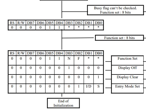
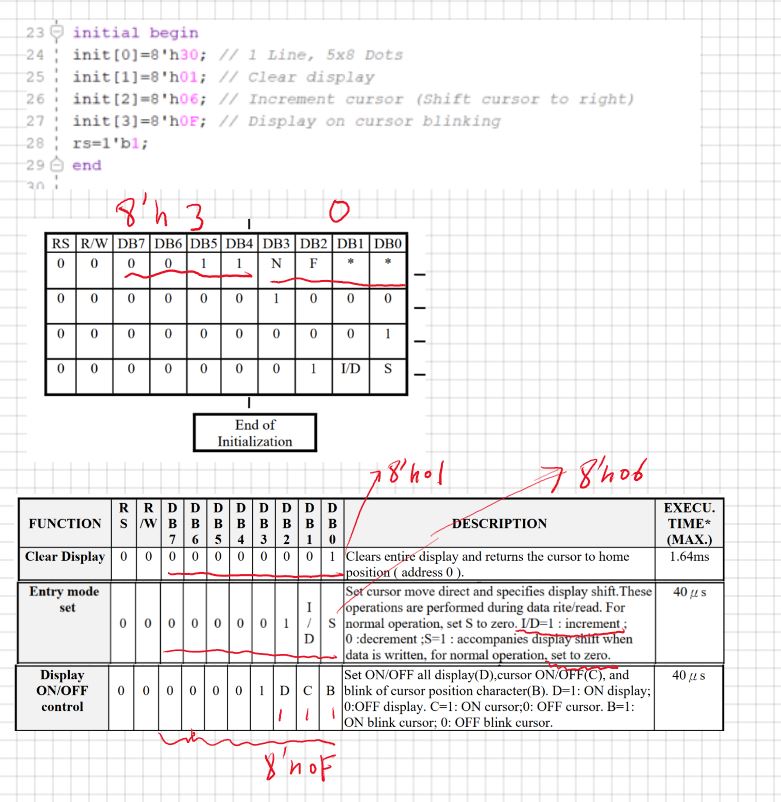
Initialization
procedure:
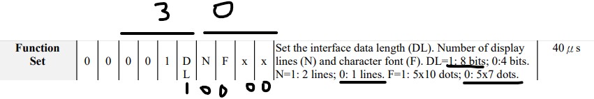
Function set -
Display off - Display clear - Entry mode set
Let's take the
function set for example:
The example code
in this tutorial:
Function set -
Display clear - Entry mode set - Display on (It seems to be
5x7 dots not 5x8)
The
order of the settings doesn’t matter that much because the 1s are
placed on the diagonal, so each function entry is controlled by a
specific range of numbers.
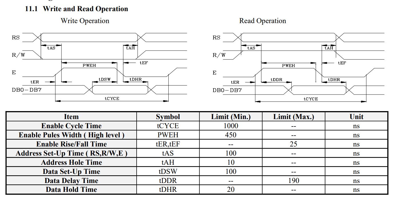
Refer to the
following timing diagram. For RS an R/W:
RS = 1, write to DR
RS = 0, write to IR
R/W = 1, read
R/W = 0, write
The
timing diagram shows that we should set the RS and R/W pins to
appropriate values (seems that RS and R/W are synchronized) and wait
for tAS before setting the E pin to logic high. Then
the E signal should have a high-to-low edge which starts a write
operation. Note that tDSW before this edge the data must be valid.
After the falling edge of E, the control signals and the data
should not change for some time denoted by tAH.
Another important issue is the “Enable Cycle Time” which should be
greater than 1000 ns. This shows that we should wait for some time
before starting to do the next read or write operation.
Summary:
Rising Edge: The
Enable (E) pin goes HIGH, allowing the internal logic to prepare to
receive data. The address/data pins (DB0-DB7) must be stable before or
at this point.
High Time: E
stays HIGH for a specific time (minimum ~450 ns).
Falling Edge: As
E moves from HIGH to LOW, the LCD latches the data currently present on
the data bus.
Write Operation:
The write operation completes when the E signal is dropped to LOW. Data Latching:
The data/command is formally read by the LCD on the falling edge.
Setup/Hold Time:
The data on DB0-DB7 must be set up before the rising edge and held
until after the falling edge of the Enable pulse.
Commands vs.
Data: This "falling edge" rule applies to both sending commands (e.g.,
DDRAM address) and data characters.
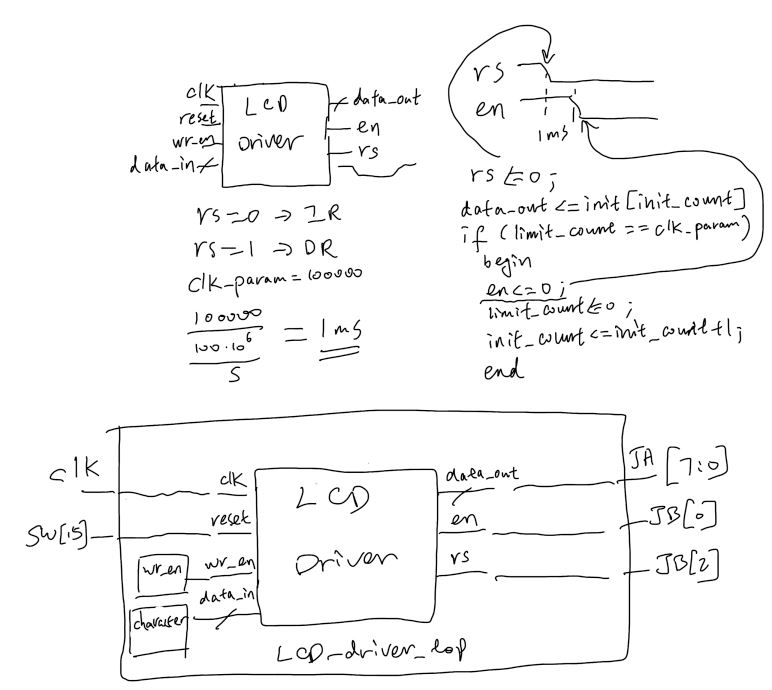
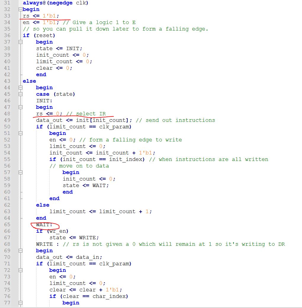
The LCD_driver.v
example provided by the textbook uses 1 ms delay before the 'en' pin to
be pulled down to ground which is an overkill (only requires about 550
ns). However, it is a good example for this lab.
'rs'
is set at '1' every time negedge of clk arrives. In the INIT state, rs
is pulled down to ground so it writes data_out to IR; In the WRITE
state, rs is not pulled down to ground which means the rs==1 will
remain unchanged so it writes to DR.
Task
1: Repeat the work on the textbook (20 points)
Task
2: Modify the code to show steady texts on the display (20 points)
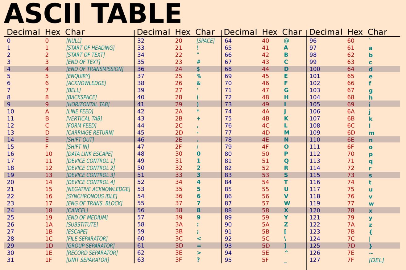
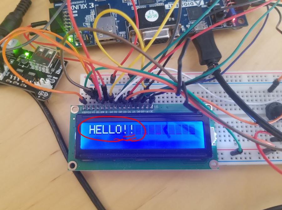
Task
3: Use ASCII code instead of letters in the code to display 'Hello !!'.
(20 points)
Task
4: Use Lab4's adder/subtractor circuit, display the addition or
subtraction operations with numbers and results on the LCD monitor. For example if the switch inputs are 001 + 010, the LCD shows '1+2', then you use a switch to show the results as '1+2=3'. For 100 + 110, the LCD should show '-4 + -2', then after the switch is toggled, it shows '-4 + -2 = -6'. When
cm1 is 1, it does subtractions. For input 011 and 001, LDC displays '3
- 1 = 2'. For input 011 and 101, LCD displays '3 - -3 = 6'. A template to start with. (40 points)