(Official technical document)
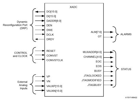
The XADC includes a dual 12-bit, 1 Mega sample per second (MSPS) ADC and on-chip sensors. The ADCs can access up to 17 external analog input channels.
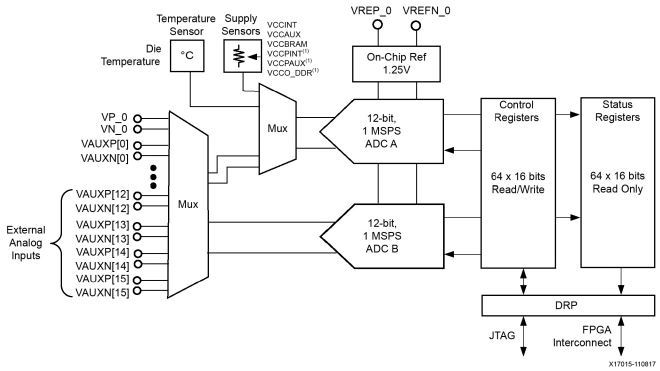
Apart from a single dedicated analog input pair (VP/VN ), the external analog inputs use dual-purpose I/O. These FPGA digital I/Os are individually nominated as analog inputs when the XADC is instantiated in a design. This document refers to these analog inputs as auxiliary analog inputs. A maximum of 16 auxiliary analog inputs are available. The auxiliary analog inputs are enabled by connecting the analog inputs on the XADC primitive to the top level of the design. When enabled as analog inputs, these package balls are unavailable as digital I/Os. It is also possible to enable the auxiliary analog inputs preconfiguration (for example, for PCB diagnostics) through the JTAG TAP
XADC ports
The ADCs have a nominal analog input range from 0V to 1V. In unipolar mode (default), the analog inputs of the ADCs produce a full scale code of FFFh (12 bits) when the input is 1V. Thus, an analog input signal of 200 mV in unipolar mode produces and outputs code of

The ADCs always produce a 16-bit conversion result. The 12-bit data correspond to the 12 MSBs (most significant) in the 16-bit status registers. The unreferenced LSBs can be used to minimize quantization effects or improve resolution through averaging or filtering. The 12-bit unipolar transfer function for the ADCs. The nominal analog input range to the ADCs is 0V to 1V in this mode. The ADC produces a zero code ( 000h ) when 0V is present on the ADC input and a full scale code of all 1s ( FFFh ) when 1V is present on the input.
The analog inputs of the ADC use a differential sampling scheme to reduce the effects of common-mode noise signals. This common-mode rejection improves the ADC performance in noisy digital environments. To take advantage of the high common mode rejection, users need only connect V P and V N in a differential configuration.

Unipolar Input Signals
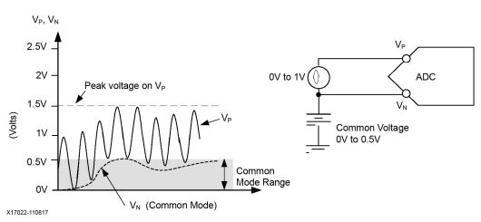
When measuring unipolar analog input signals, the ADCs must operate in a unipolar input mode. This mode is selected by writing to configuration register 0 (see Control Registers, page 35 ). When unipolar operation is enabled, the differential analog inputs (V P and V N ) have an input range of 0V to 1.0V. In this mode, the voltage on V P (measured with respect to V N ) must always be positive. Figure 2-6 shows a typical application of unipolar mode. V N is typically connected to a local ground or common mode signal. The common mode signal on V N can vary from 0V to +0.5V (measured with respect to GNDADC). Because the differential input range is from 0V to 1.0V (V P to V N ), the maximum signal on V P is 1.5V.
Bipolar Input Signals
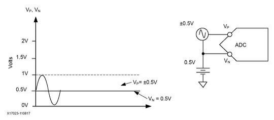
The analog inputs can accommodate analog input signals that are positive and negative with respect to a common mode or reference. To accommodate these types of signals, the analog input must be configured to bipolar mode. Bipolar mode is selected by writing to configuration register 0 (see Control Registers ). All input voltages must be positive with respect to analog ground (GNDADC). When bipolar operation is enabled, the differential analog input (V P – V N ) can have a maximum input range of ±0.5V. The common mode or reference voltage should not exceed 0.5V in this case
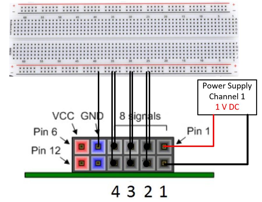
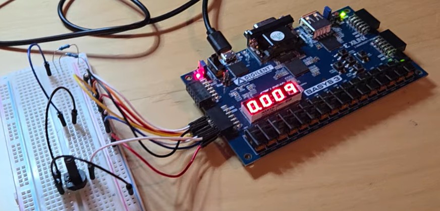
In our application, simply short GND to VN and short OpAmp output to VP. We are not lifting the output by adding an bias to it.
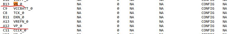
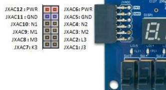
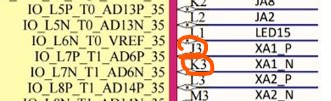
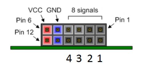
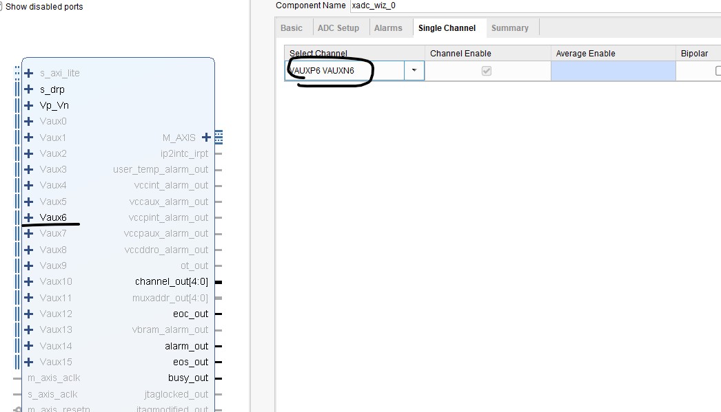
The Basys 3 board only has 4 channels of the ADC connected to header pins.

Other AD ports can be identified on the pinout of the XC7A35T - CPG236 device