Analog Signal - XADC - Basys 3 SPI - Arduino Practice
This
tutorial teaches how to integrate the XADC IP block into your FPGA
design and access the digital output and transmit them to an external
MCU through SPI.
The
analog input (AO) must be 0-1V. If you are taking CE433 and you have
the Easy Pulse Sensor module, you should use that output (adjust it to
0-1V) as AO.
The hardware connections follow. Note that AO is
connected to vauxp6; and vauxn6 is shorted to GND. The vauxp/n pins are
at the JXDC pins (bottom left of the board).
All other ADC channels are grounded to avoid noises.
GND
from Arduino is used to connect to the common GND of the entire circuit
however the VCC (5V) of Arduino shouldn't be used on Basys3 (3.3V
device). As a Leader device, the SPI module in the FPGA will send sck,
ss, and mosi to Arduino so it's a one-directional communication which
won't hurt the FPGA board.
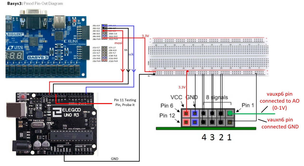
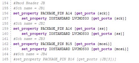
JB1 - 3 are used as sck, ss, and mosi respectfully. Follow the procedure in the XADC tutorial to add an XADC IP to this design.
The
FPGA board is now used as the leader transmitter, it outputs voltages
to the 5V logic Arduino so NO level shifter is needed in this circuit.
On the Arduino board, Pin 13 is mosi, Pin 12 is ss, and Pin 2 is sck.
Pin
11 is used as a testing pin in your C code. This is a very handy
technique to debug your circuit. If you are taking my MCU class in the
fall, you will use this technique quite often.
This is how Pin 11 creates a pulse to indicate that this piece of code is executed.
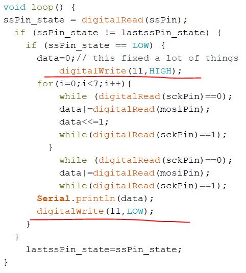
The complete Arduino code. Note that the two first two lines of code right below the for loop seem to be unnecessary, test it and let me know.
Here
is the observation. The mosi line comes from the FPGA. I wrote a
constant value 8'b00001111 to the mosi output from the FPGA for
debugging purposes.
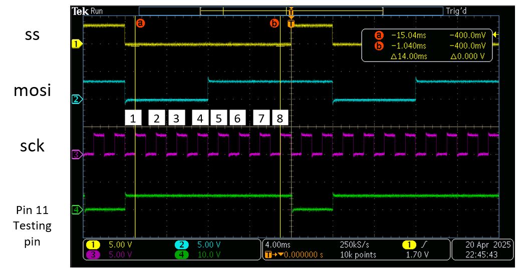
In the SPI_leader_transmitter.v code,
at the negedge of the sck, ss is pulled down to 0 at the same time to
enable the follower device. From the observation above, at the left
handside of the label '1'. The falling edge of sck, mosi, and ss almost
happened at the same time. Waiting for a half sck cycle to sample the
data on the mosi line at the rising edge of the sck clock will be
perfect (the yellow cursor labeled '1' or 'a' samples a '0' from mosi).
The 'a' cursor samples a 0 from mosi, and this 0 is the MSB of the byte
'8'b00001111' sent through the FPGA.
After
sck rising edge No. 1, you can count to 8 sampled bits by Arduino
and the 8th rising edge is right before the 'ss' enable line got pulled
up to disable the transmission. This signals the completion of
transmission of 1 entire byte.
The Testing pin is pulled up and down at the correct time points which indicates that the Arduino code is executed as expected.
Observing
the output from the FPGA should be the first step of this project since
we need to know that the SPI leader transmitter module is functioning
before moving on.
I
connected the entire circuit to Arduino and observed the output to the
Serial monitor. I received '15' constantly there so this is great
news.(8'b00001111).
Here is how I output a constant data to mosi.
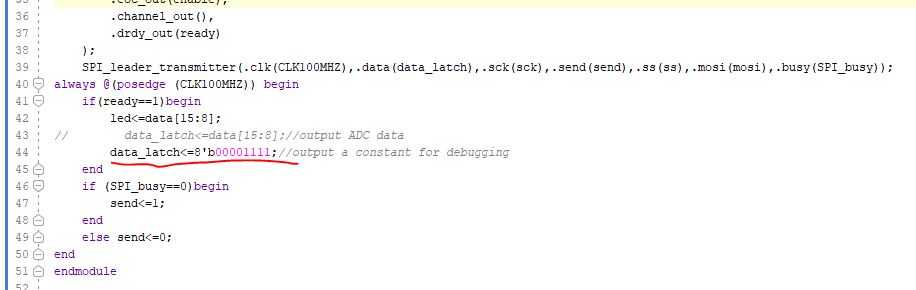
Code for the top module main.v
The constraint file.
Switch it back to the commented one above will deliver ADC outputs to mosi.
--------------------------------------------
Final deliverables and rubric
Task 1:
XADC
outputs constant data (8'b00001111) to an oscilloscope. If you
oscilloscope only has two channels, please display sck and mosi. (25
points)
Task 2:
Use
the Easy Pulse Sensor as AO. Signal outputs to an Arduino IDE in the
Serial plotter. Show you verilog and Arduino code. A video demo is
required for the report. (25 points)