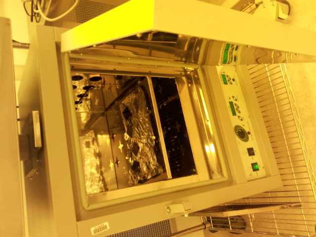
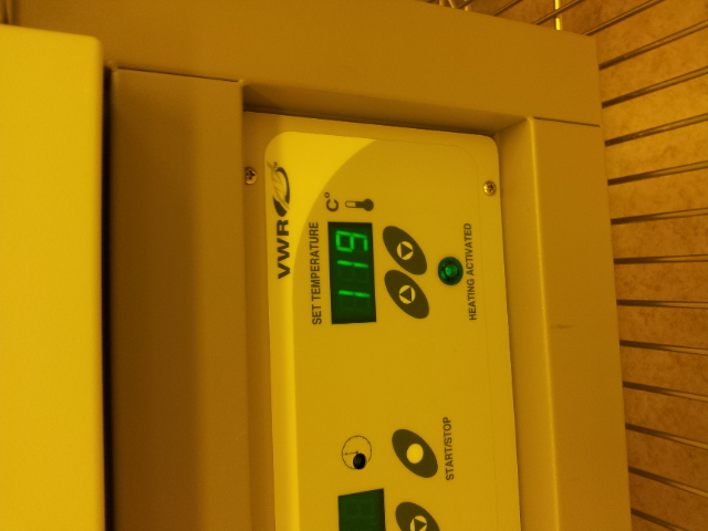
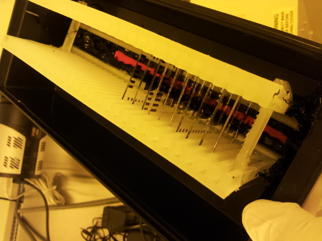
The experiment protocol is briefly described here. Some of the figures are attached.
It
is fabricated in the cleanroom facility of Nevada Nanotechnology Center
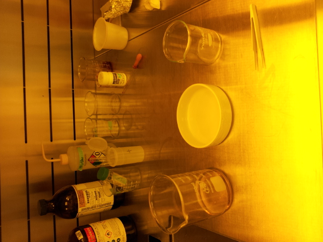
at University of Nevada, Las Vegas. The fabrication reagents includes
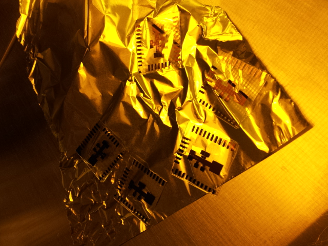
Schott Boro Float glass substrate with Chrome coated (100 nm)
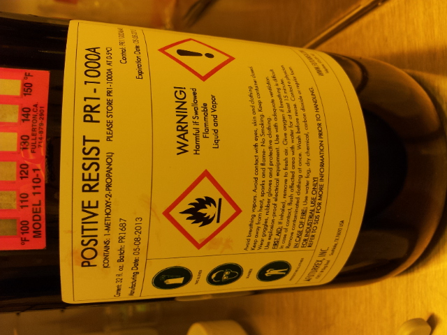
microfluidic blank slides (with positive photoresist coated, Telic,
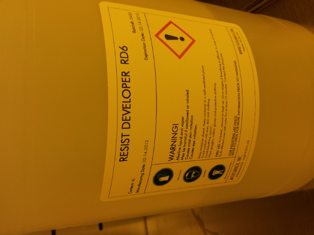
Valencia, CA, USA), photoresist developer RD6 (Futurrex, INC.,
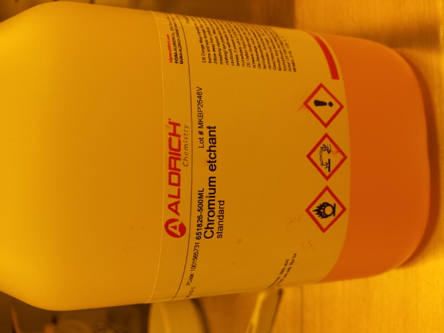
Franklin, NJ, USA), Chromium etchant (Sigma-Aldrich, Co., MO, USA) and
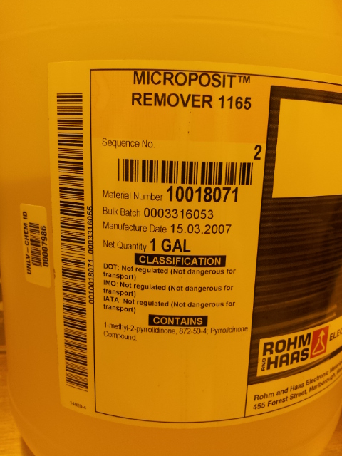
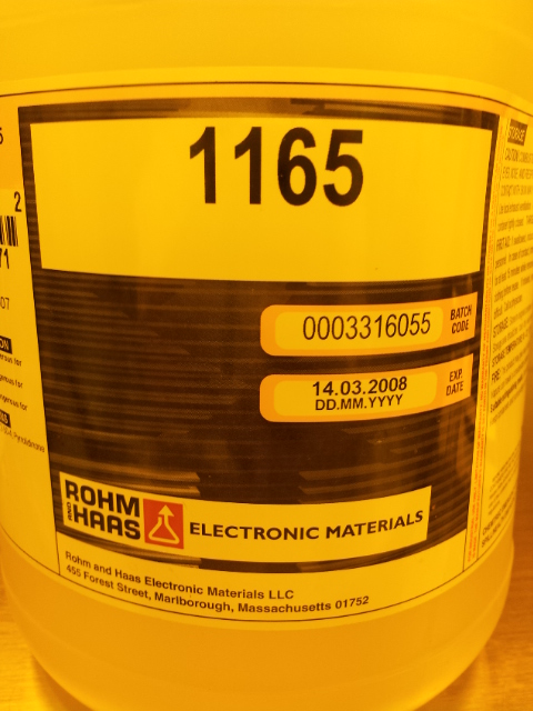
photoresist remover (Microposit Remover 1165, Rohm and Haas Electronic
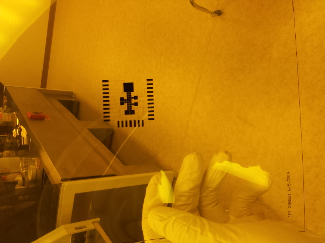
Materials LLC, MA, USA). Open source integrated circuit (IC) layout
tools Electric VLSI is used to pattern the mask of the electrode array.
GDSII output files from Electric VLSI were sent to Infinite Graphics
INC. (MN, USA) for plotting (25,000 dpi resolution) on a plastic
photolithography film.
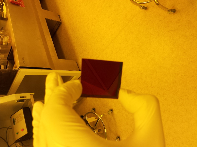
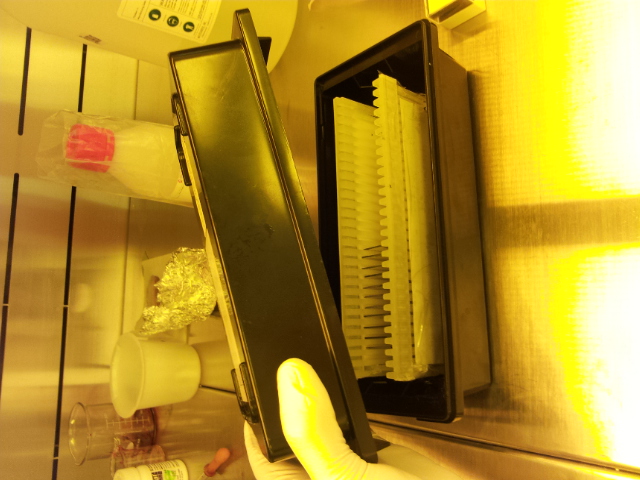
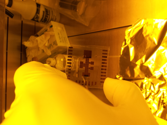
The substrates are covered by the patterned
photomask and exposed to a UV light source for 45 seconds and then
developed for 1 min in RD6. Substrates are then immersed in the
Chromium etchant for about 15-20 seconds. Then the substrates are
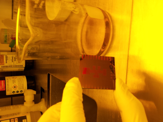
washed by DI water and dried out using nitrogen gas. The remaining
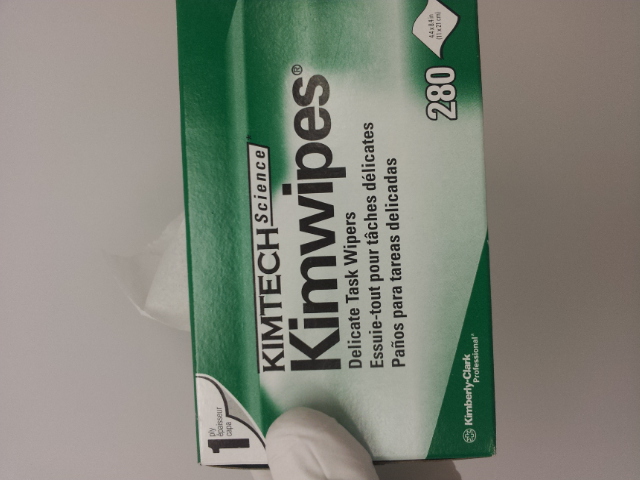
photoresist is removed by Microposit Remover 1165. If the remover
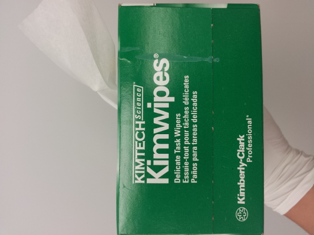
doesn't remove all of the photoresist Kimwipes (Uline, WI, USA) (wetted
by Microposit Remover or DI water) can be used to remove the remaining
photoresist.