Tutorial 3:
Self-Defined Libraries
(Selected materials from autodesk.com)
In Autodesk EAGLE, all of the parts that you place on your designs
are stored in libraries. These provide an easy way to keep parts
organized based on their category. For example, you might have a
library for a general category like capacitors. Or specific communities
like Sparkfun have their own dedicated libraries that contain a variety
of parts for specific projects. Libraries and the parts within are
connected in a simple hierarchy in Autodesk EAGLE. This makes it easy
to understand how everything’s connected. Here’s how it’s organized:
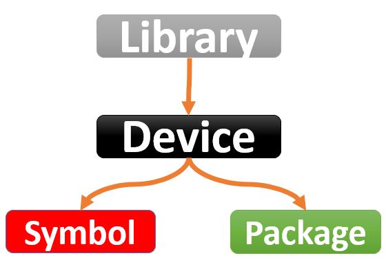
-Libraries.
All
of your parts will be stored in your personal library folder in
Autodesk EAGLE. Each part will contain a device, symbol, and package.
-Devices.
Within
every library, you’ll have one or multiple devices. These devices
include both a schematic symbol and a package in one accessible
location.
-Symbols.
Within every device, you’ll have a symbol, which provides a visual
representation of a part for use on a schematic.
-Packages.
Within every device, you’ll also have a package, which is the physical
representation of a part for use in a PCB layout.
When
you put all of these pieces together, you’ll get a tree structure that
shows off how libraries in Autodesk EAGLE are organized. Check it out
below.
Creating Your Library
Now
that you understand how libraries work in Autodesk EAGLE, it’s time to
make your own! You can skip this step if you already have your personal
library folder, otherwise:
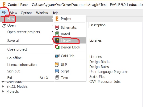
-Open Autodesk EAGLE, and you’ll be greeted with the Control Panel.
-Next, select File » New Library to open your Library Window.
-Before
creating any new parts, you need to save your library by selecting File
» Save (or Cmd + S on Mac and Ctrl + S on Windows)
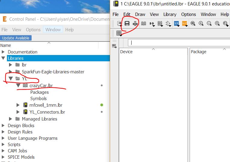
-Now that
your library is saved, you just need to activate it. Go back to your
Control Panel, right-click your new library, and select Use. You’ll
know if your library is ready to go if it has a green dot next to it in
your Control Panel.
The
.lbr file will be the library file that contains Devices. Every device
is a combination of a 'symbol' and a 'package'. A symbol can have many
packages (layouts) since the same symbol can be used to represent many
types of layouts like SMT or DIP. However, every package usually only
has one symbol to represent it in the schematic. Keep in mind that, the
schematic is just a symbol to represent the role of an electrical
component in a circuit, it does not have to changed all the time unless
necessary.
You can put your .lbr file (includes devices,
symbols, and packages) into different folders. You can even have
subfolders for these folders to host your .lbr files.
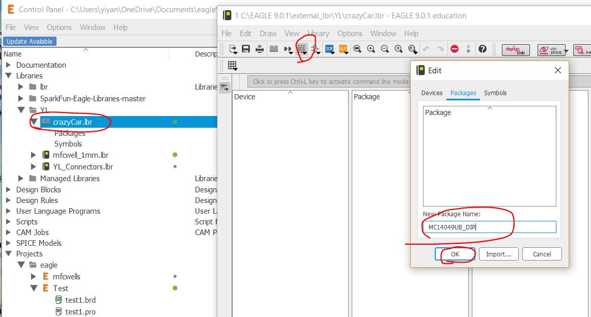
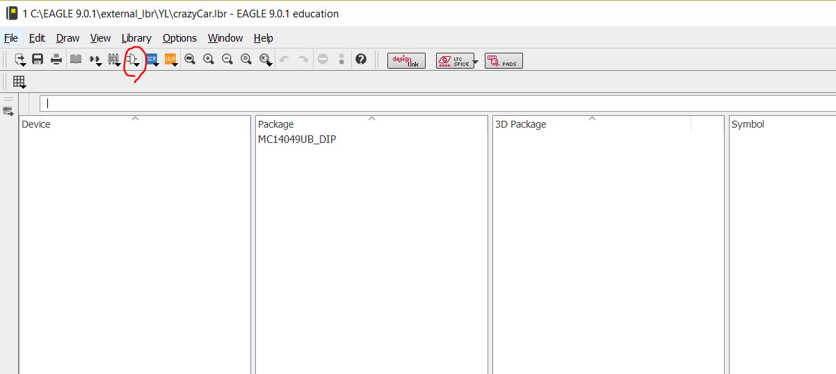
I
created a folder called YL in the 'Libraries' menu. After I had my
library window pops up, I saved it to my 'YL' folder, and I named it as
'crazyCar.lbr'.
Library Basics Part 1: Creating Your First Package
Packages
serve a super important purpose when used on your PCB layout, offering
a set of pads that provide both electrical connectivity and a way to
solder parts onto your board. As you can imagine, making sure these
pads are placed exactly where they need to be is a necessary challenge;
otherwise, you’ll get a board back from manufacturing that doesn’t
work! Check out the image below of the package you’ll be creating
today. Here are all of the elements that you will start to work with:
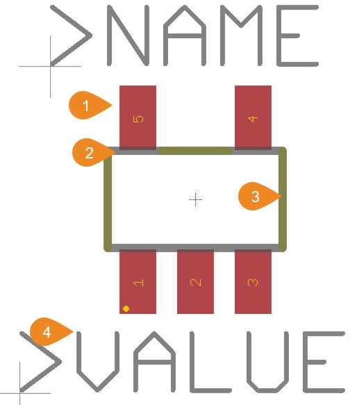
1. Pads.
The pads are the red rectangles on this part and are numbered according
to your datasheet. When placed on a PCB, each of these pads will be
connected to a trace and provide electrical connectivity for a part.
2. Package Dimension.
The package dimension is the rectangular gray outline that you see
connecting all of the pads. This outline represents the actual physical
dimensions of your part can help during your PCB layout process to see
if you’re placing components too close together.
3. Silkscreen Outline.
The silkscreen outline is the rectangular yellow lines lying over the
gray package dimension lines. While this piece is optional, it helps to
provide a visual indicator for your manufacturer when they are
assembling parts on your bare board.
4. Name and Value. These
text elements are placeholders and will come in handy during your PCB
layout stage. As the text suggests, Name will be used to identify the
unique name of your part when you place it on your PCB layout, and
Value can be utilized for things like labeling the resistance of a
resistor, capacitance of a capacitor, etc…
Step 1 – Creating Your
New Package
Alright,
time to get rolling with the tutorial part of this guide. The very
first step you need to complete is creating a new package in your
library. Here’s how: Open Autodesk EAGLE, and you’ll be greeted with
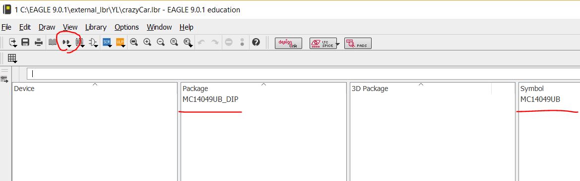
the Control Panel. Select the Arrow icon to expand the main Libraries
and lbr folders, then right-click your personal library and select
Open. This will open your Library Window. From here, choose the Package
package-icon icon to open the Edit
Dialog.
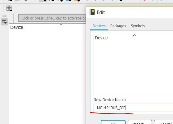
Next, enter a name for your package in the New field and select OK. If
you’re following our example, then enter “MC14049UB_DIP.” Select Yes to
confirm you want to create the new package.
Let's start with the
'package'. Double click the crazyCar.lbr in the control panel to open
the library window. Single left click the 'package' button, copy and
paste the name 'MC14049UB_DIP' in the
Edit window.
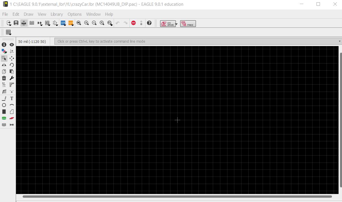
Great,
so with that complete you now have your first very package added to
your personal library and a blank Package Editor should be open as
shown below.
Step 2 – Changing Your
Grid Size
Now’s
the time to tweak some basic grid settings before you start placing any
pads. Changing the grid size will allow you to quickly and precisely
place pads according to your datasheet measurements.
-Select the Grid grid-icon icon in the top-left corner of your
interface.
-In the Grid dialog, change your Display from Off to On if it isn’t
already enabled.
-Next, change your Size: from inch to mm, and enter “0.5” as the
value, use '0.05' for Alt.
-Select OK to save your grid settings.
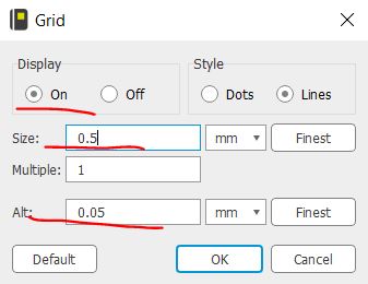
The
'Alt' function is really nice. If you setup the main grid to be 0.5 mm,
sometimes it is anoying since you cannot make small movements with the
components. The Alt grid is the secondary grid which only start working
when you press the 'Alt' key on the keyboard when you are moving the
components.
After confirming your settings, you might notice
that you can’t see your grid in the package editor. It’s not gone! You
just need to zoom in a bit with the Zoom in zoom-in-icon icon until it
becomes visible again.
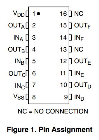
Step 3 – Deciphering Your
Datasheet
Alright, time for some datasheet detective work. Open your MC14049UB_D.PDF
datasheet and head on down to the Land Pattern Data section on page 25.
This page will give you all the information you need to precisely place
your pads. Here’s what you need:
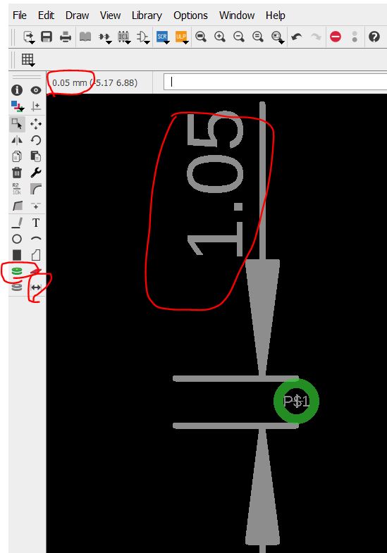
Through-holes: The unit of the value
beside
the Dimension/Scale bar is mm (mili meter). Check the unit and scale of
the grid on the left top part of the window (0.05 mm here). The green
ring sybmol highlighted on the left is the through-hole. The current
diameter of the through-hole is 1.05 mm.
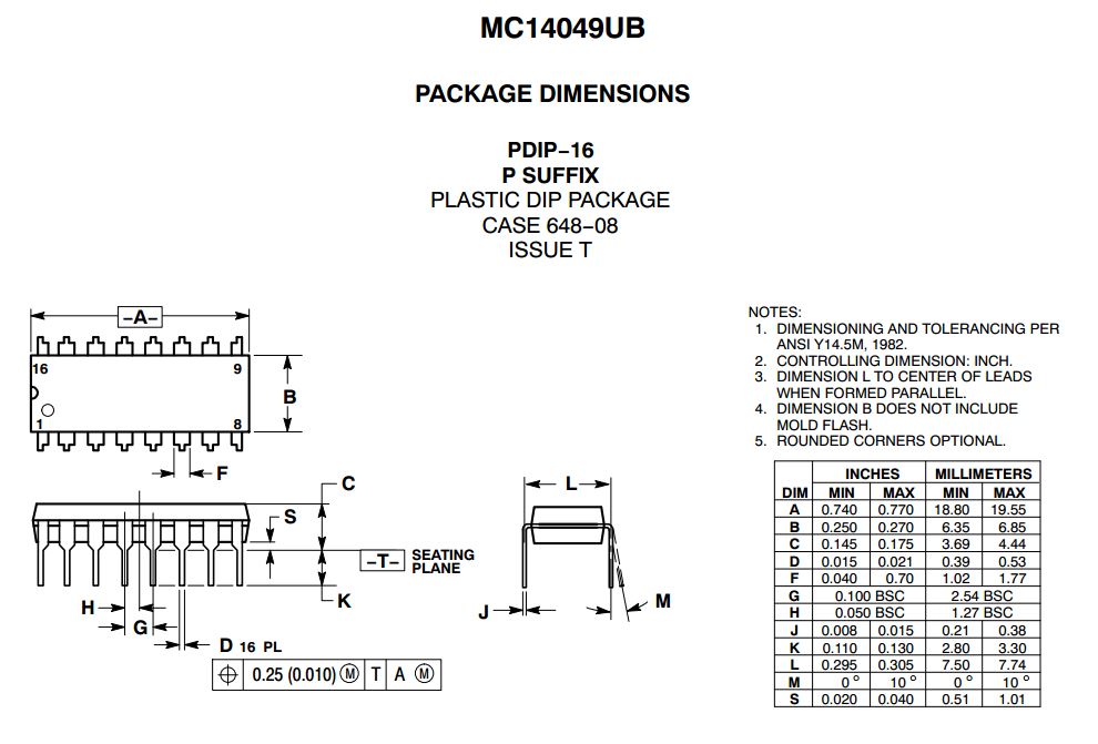
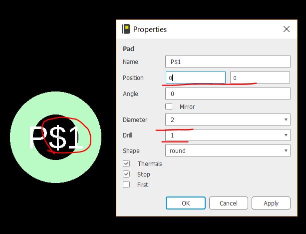
Looking
at our datasheet in
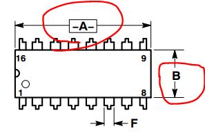
page 5. Refer to the dimension entry 'D'. The width of the pin
is 0.53
mm, but we usually set the diameter of the hole to be 1 mm in this case
to make sure the pin can be inserted into the hole. Right
click the center of the through-hole, select 'properties', set the
coordinate of the ring to be '0, 0', and the drill to be 1 mm, the
diameter to be 2 mm.
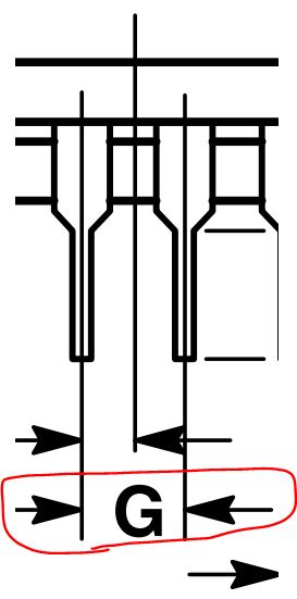
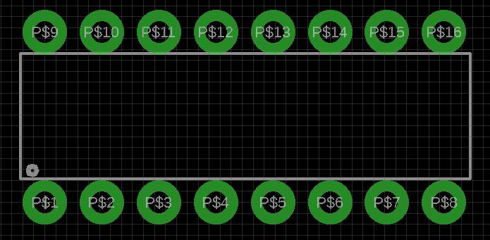
Now,
we need 2x8 of these through-holes for the 16 pins of the chip. The
distance between each two pins on the same side is the dimension of 'G'
(2.54 mm, let's use 2.6 mm). The distance of the two pins across the
chip is the dimension of 'L' (7.74 mm, let's use 7.8 mm).
Copy
the first ring and paste it beside it. Right click the second ring and
set the coordinate at 2.6, 0, so the distance is set to 2.6 mm.
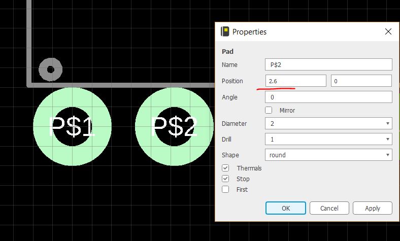
Repeat this until you have 16 evenly distributed rings (through-holes).
This will tell the PCB manufacturer to drill 16 holes using your
defined layout onto the PCB board.
Step 4 – Adding Your
Origin Point
You’ll
need to add an origin point to Pad 1 so that your manufacturer knows
the correct way to orient your part during assembly. Here’s how to do
this:
-Select the circle icon on the left-hand side of your interface.
-Select the width: dropdown at the top of your interface and select 0.
-Select the layer dropdown at the top of your interface and select
layer 21 tPlace.
-Left-click in the bottom-left corner of Pad 1 and drag your cursor to
the right to adjust the size of your circle.
-Left-click again to confirm the size of your circle and place it.
The
size of your origin point is totally up to you. All that’s important is
that it’s on Pin 1 so your manufacturer knows how to orient your part.
If you need to move your origin point, use the Move move-icon tool.
Step 5 – Adding Your
Package Dimension
You
now need to add a package dimension, which will help you to see if your
parts are placed too close together on your PCB layout. This process
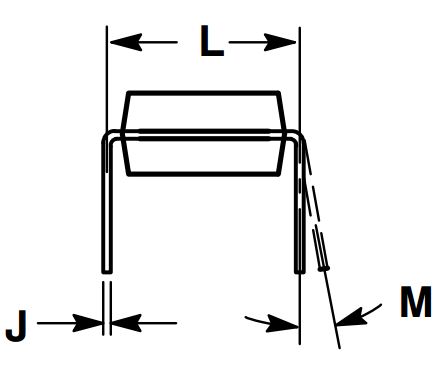
again requires some brief datasheet detective work. The dimensions are
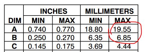
'A' and 'B', which is about 19.6 mm, and 6.9 mm.
-Select the Line wire-icon icon on the left-hand side of your
interface.
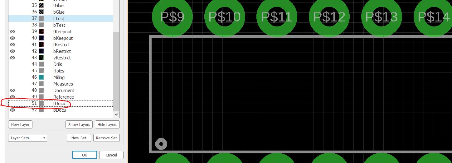
-Select the Layer dropdown at the top of your interface and choose
layer 51 tDocu.
The final result looks like this:
Step 6 – Adding Your Silkscreen Outline
Now
you just need to add a silkscreen outline, which is a helpful way to
tell your manufacturer where your part will be placed. Here’s how to do
it: Select the wire-icon on the left-hand side of your interface.
Select the Layer dropdown at the top of your interface and choose layer
21 tPlace. You now need to draw silkscreen wires on top of your package
dimensions.
The silkscreen and the dimension layer have the same color. To make
sure your silker screen layer is done, go to 'View - Layer Settings',
to uncheck the 'eye' in front of 'tDocu' to make the 'tDocu' layer
invisible. If you are still able to see the rectangular shape like I
have below, you know that the silker screen layer is ok.
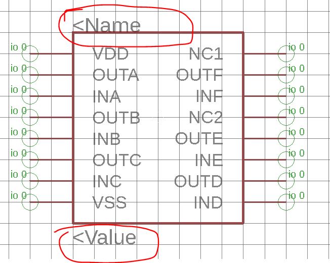
Step 7 – Adding Your Name and Value Placeholders
Alright,
time to finish this up! The last thing you need to add is both a name
and value placeholder to your package. This will allow EAGLE to create
a unique identifier for each and every part on your PCB layout, making
it easy to reference specific parts if you need to make changes down
the road. Let’s do it:
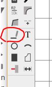
-Select the Text text-icon icon on the left-hand side of your interface.
-In the Text Dialog, enter “>NAME” in the Enter text: field and select OK.
-Next, select the Layers dropdown at the top of your interface and choose layer 25 tNames.
You’ll
know that you put your >NAME text on the right layer if it displays
in a gray colored font. Go ahead and repeat the steps above, this
substituting >NAME for >VALUE on layer 27 tValues and place it on the bottom of your package. Here’s how your completed package should look:
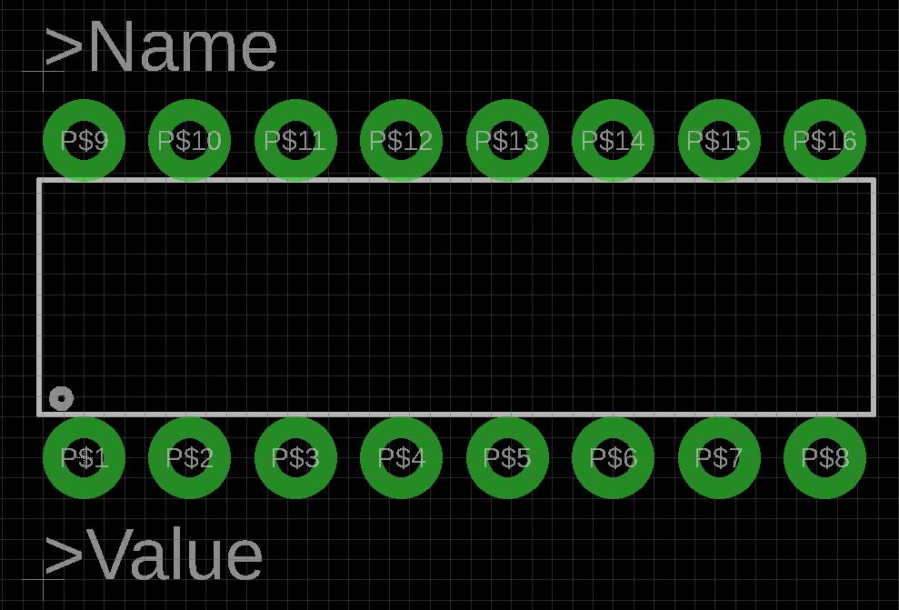
At last, you’re done! This is how your completed package should look with its new name and value placeholders.
Library Basics Part 2: Creating Your First Symbol
Now,
it’s time to continue on your journey by learning how to build your
first symbol. Regardless of what kind of design you’re creating, it all
begins with symbols and schematics. You can think of these symbols as
the map to the chest of schematic treasure! Symbols show off all the
functionality of your design without having to get into the nitty
gritty of physical dimensions and packages.
Find the Pin configuration of the chip from the datasheet:
Step 1 – Creating Your First Symbol
If
you haven’t already done so, go ahead and open your library from the
EAGLE Control Panel. You can do this by right-clicking on the name of
your library and selecting Open. This will open the Library Window,
which provides a summary of all the devices, packages and symbols in
your personal library. To add a new symbol to your library:
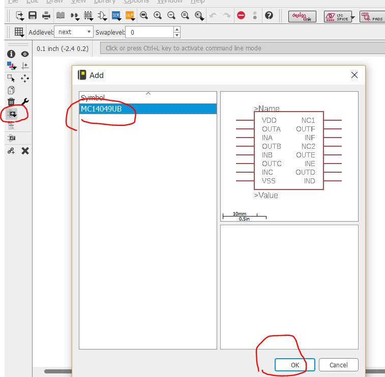
-Select the Symbol open-symbol-icon icon at the top of your interface to open the Edit Dialog.
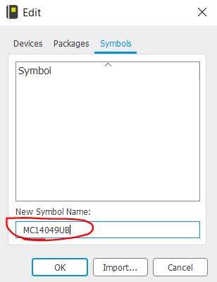
-Next, enter a name for your symbol in the New: field and select OK. In our example, we’ll give our symbol a name of “MC14049UB_DIP”
-A warning dialog will open, select OK to confirm that you want to create the new symbol name.
Close
the Package edit window, and reopen the library edit window from the
control panel as above. Click the 'Symbol' button in the menu.
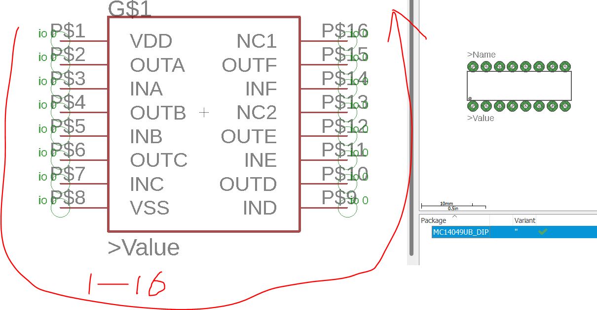
We name the symbol 'MC14049UB' instead of 'MC14049UB_DIP'
here as the package since the same sybmol may have different packages.
If the other package is an SMT layout, then you may want to name it as 'MC14049UB_SMT'. But they both can share the same symbol, which is 'MC14049UB'.
Zoom out the window, you can see the origin cross:
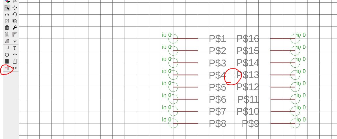
Step 2 – Adding Pins to Your Symbol
Let’s insert some pins to your symbol.
-Select the Pin pin-icon icon on the left-hand side of your interface.
-Left-click in your Symbol Editor workspace to place your first pin.
-Go
ahead and repeat this process for the remaining pins on your symbol. To
place the 2 pins on the right, right-click twice to rotate your pin
180° and then left-click to place.
We’ve left a gap between
ours for easier readability as shown in the image below. But those pin
names aren’t right; we will change those now.
Try the best to make the origin cross in the middle of your symbol. I circled the origin in the snipshot above.
Step 3 – Changing Your Pin Names
You
probably noticed that Autodesk EAGLE names all of your pin names by
default as you place them. But we need to change these to match what it
shows on our datasheet. To do this:
-Select the Name name-icon icon on the left-hand side of your interface.
-Select the first pin you placed, and the Name dialog will open.
-Enter “VDD” in the New Name: field and select OK.

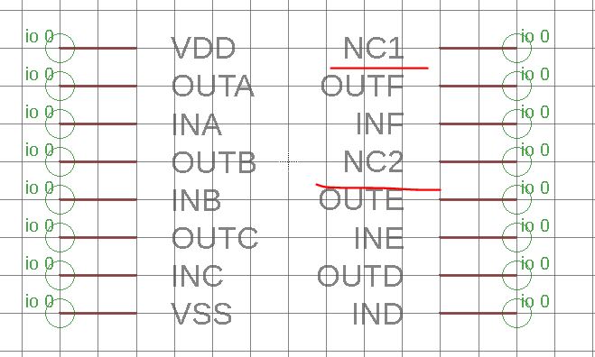
Please
note that, NC1 and NC2 are both the NC pin on the chip. This pin will
not be used, or 'No Connection'. Eagle does not allwo you to have two
pins using the same name. This is why I name them diffrently.
Step 4 – Adding Your Symbol Outline
To
complete the visual of your symbol, you’ll now need to add an outline
to group all of your pins together. Here’s how to accomplish this:
-Select the Line wire-icon icon on the left-hand side of your interface.
-Next, left-click on a starting point to begin drawing your outline.
-Continue to drag and left-click as needed to complete each side of your outline to draw a full box.
Use the 'T' button to add Text '>Name' and 'Value' to the sybmol.
Library Basics Part 3: Creating Your First Device in Autodesk EAGLE
In
this guide, we’ll be pulling together everything you learned about
creating a package in Library Basics Part 1 and creating a symbol in
Library Basics Part 2. Now, it’s time to create your very own device.
You’ll be able to do the PCB design with a brand new part.
Step 1 – Creating Your New Device
Creating
a new device follows a familiar set of steps that you should be used to
by now after creating a package and symbol. Close the Symbol edit
window, enter the library windwo again from the control panel.
Click the 'Device' button, name it as 'MC14049UB_DIP'.
Step 2 – Adding Your Symbol and Package
Add the symbol:
Adding Your Package:
Select the New button on the bottom-right corner of your Device Editor.
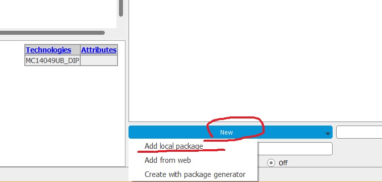
Select OK, and your package will automatically be placed on the right panel of your Device Editor.
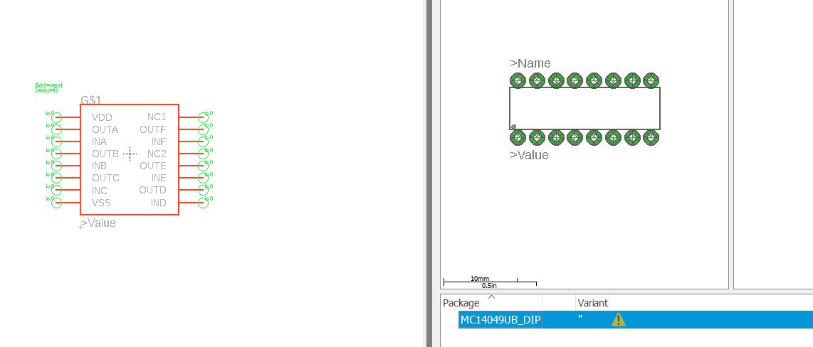
Looks
exciting!! Now, let's connect the symbol to the physical layout
(package). After click 'Connect', the window as follows will pop up to
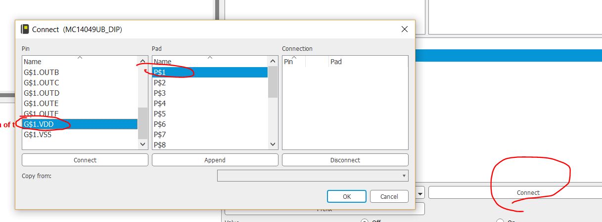
let you match the corresponding pins in the symbol and in the layout.
Pin 1 is VDD, so I select these two in the two windows, and then click
connect.
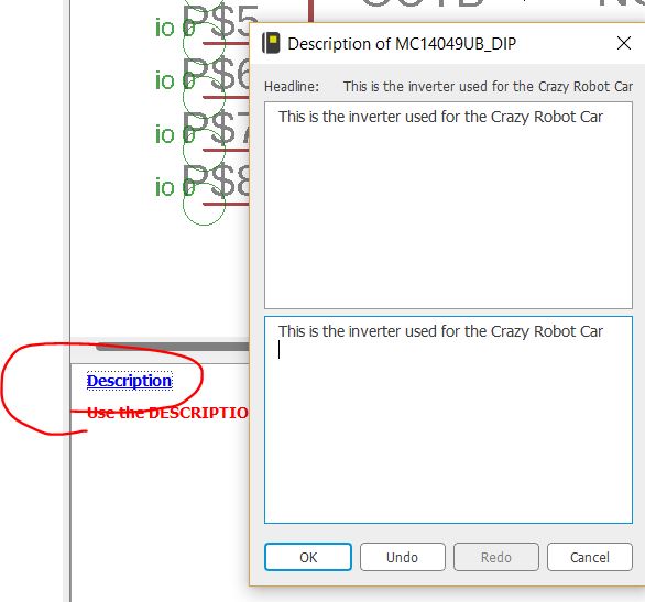
Add some descriptions. We did not make the description very professional since our project is simple.
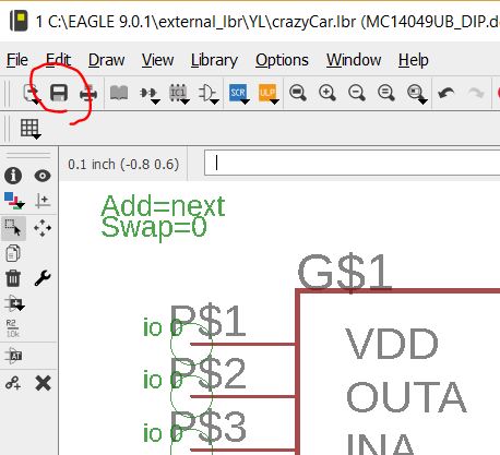
Don't forget to save it before you close it:
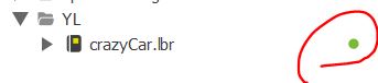
Also, don't forget to have Turn ON your library:
Now, you can directly use your parts in both the Schematic view and the Layout View to complete your circuit.
Use the same mathod to design the library (Device, Symbol, and Package) for the Motor Driver L293D.
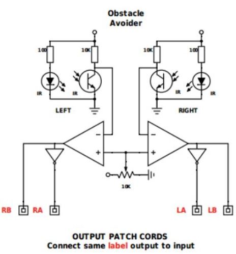
The schematic of the Obstacle Avoider is:
All
the other components are 'Two Terminal' components, which are easy. You
can build the libraries for them as well. Or probably just make one
package, and call it 'Two_Termi', and then design different symbols to
connect them to this package to make different devices.