This tutorial is the first of a two-part Using EAGLE series, and it’s devoted entirely to the schematic-designing side of EAGLE. In part 2, Using EAGLE: Board Layout, we’ll use the schematic designed in this tutorial as the basis for our example board layout.
If you’d like to follow along with this tutorial, make sure you’ve installed and setup the EAGLE software. The Tutorial 1 'PCB Basics' covers the basics of what EAGLE is and what makes it great. It also covers how to download and install the SparkFun EAGLE libraries we’ll be using in this tutorial. Definitely read through that tutorial before you continue on.
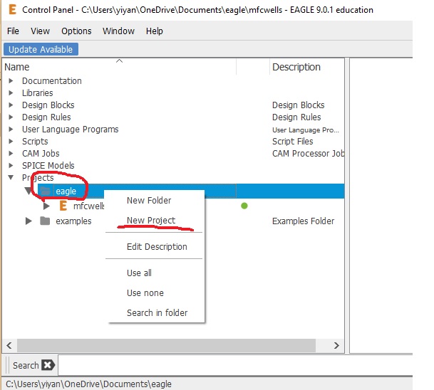
Create a Project We’ll start by making a new project folder for our design. In the control panel, under the “Projects” tree, right click on the directory where you want the project to live (by default EAGLE creates an “eagle” directory in your home folder), and select “New Project”. You can see in the figure below, I have my project 'mfcwells' already sits there.
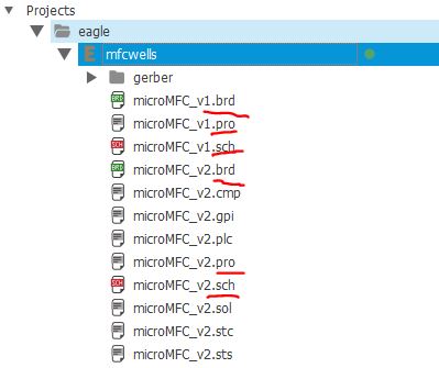
I expand the drop down menu of my 'mfcwells' project, you can see that, for the same project, you can have many Schematics and Boards in it (.brd is the board layout, .pro is the project file, .sch is the schematic file). This makes perfectly sense. Think about that you have a massive project called the 'Laptop Mother Board', you may have many of the functional modules on the board, for example the power supply module, the DRAM module, and the Video Card module, etc. These modules have very limited connections (probably only share the same power supply) but they do belongs to the same project - the 'Laptop Mother Board' Project. You'd like to put them into one project in order to organize them well.
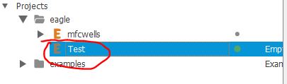
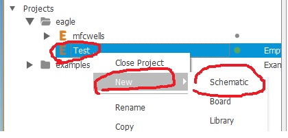
Let's create a project called Test.
Right click the Test project, and select New - Schematic
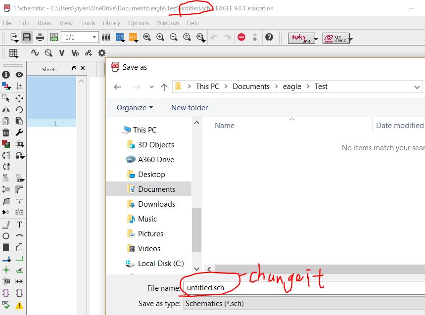
In the beginning, you can find the name of this new schematic is 'untitiled'. You may want to change it to a different name before you move forward. Keep in mind that, a single project can have many schematics. I named it as 'test1'. It's better to make the name without spaces and unusual symbols.
Adding Parts to a Schematic Schematic design is a two step process. First you have to add all of the parts to the schematic sheet, then those parts need to be wired together. You can intermix the steps – add a few parts, wire a few parts, then add some more – but since we already have a reference design we’ll just add everything in one swoop.
Using the ADD Tool
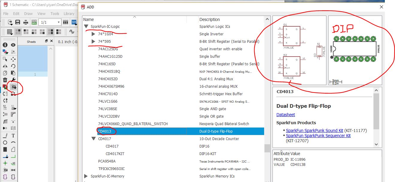
The ADD tool – (on the left toolbar, or under the Edit menu) – is what you’ll use to place every single component on the schematic. The ADD tool opens up a library navigator, where you can expand specific libraries and look at the parts it holds. With a part selected on the left side, the view on the right half should update to show both the schematic symbol of the part and its package. (Press Ctrl + A will do the same job).
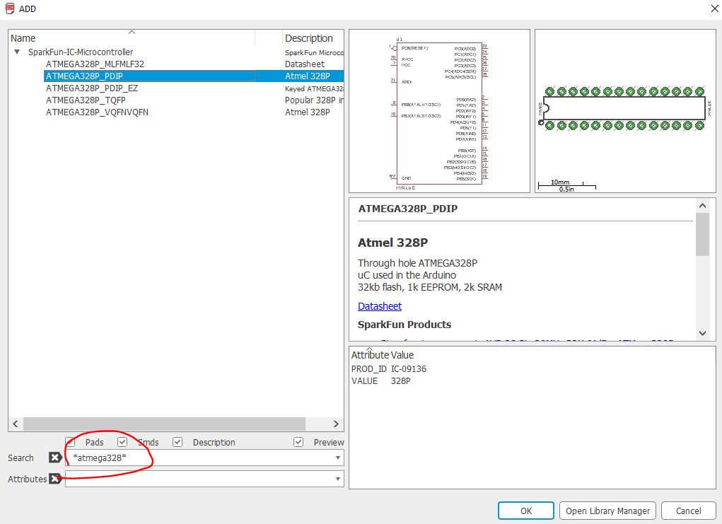
For example if I select CD4013, on the right side of the window, you will see the chip's schematic view and its layout view. The layout view shows the outline of the chip, and the PADS of the chip. If you see circle pads, that means this layout is for DIP IC packages, there will be through holes being drilled on the bowrd in order to insert the chip into it and get it soldered.
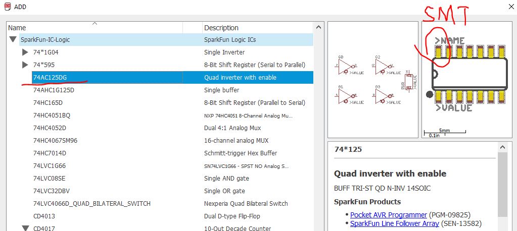
If you see the layout view like the following one, then it is a 'SMT (surface mount)' layout. No holes will be drilled on the board, and you need to buy the corresponding SMT version of the IC to fit to this layout.
We are not adding these two chips to our circuit but just show you two examples.
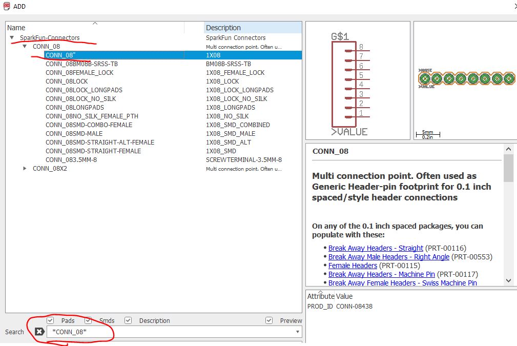
The ADD tool also has search functionality – very helpful when you have to navigate through dozens of libraries to find a part. The search is very literal, so don’t misspell stuff! You can add wildcards to your search by placing an asterisk (*) before and/or after your search term. For example if you search for atmega328 you should find a single part/package combo in the SparkFun-DigitalIC library, but if you search *atmega328* (note asterisks before and after), you’ll discover two more versions of the IC (because they’re actually named “ATMEGA328P”). You’ll probably want to get accustomed to always adding an asterisk before and after your search term.
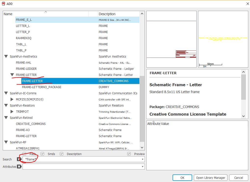
Step 1: Add a Frame
The frame isn’t a critical component for what will be the final PCB layout, but it keeps your schematic looking clean and organized. The frame we want should be in the SparkFun-Aesthetics library, and it’s named FRAME-LETTER. Find that by either searching or navigating and add it to your schematic.
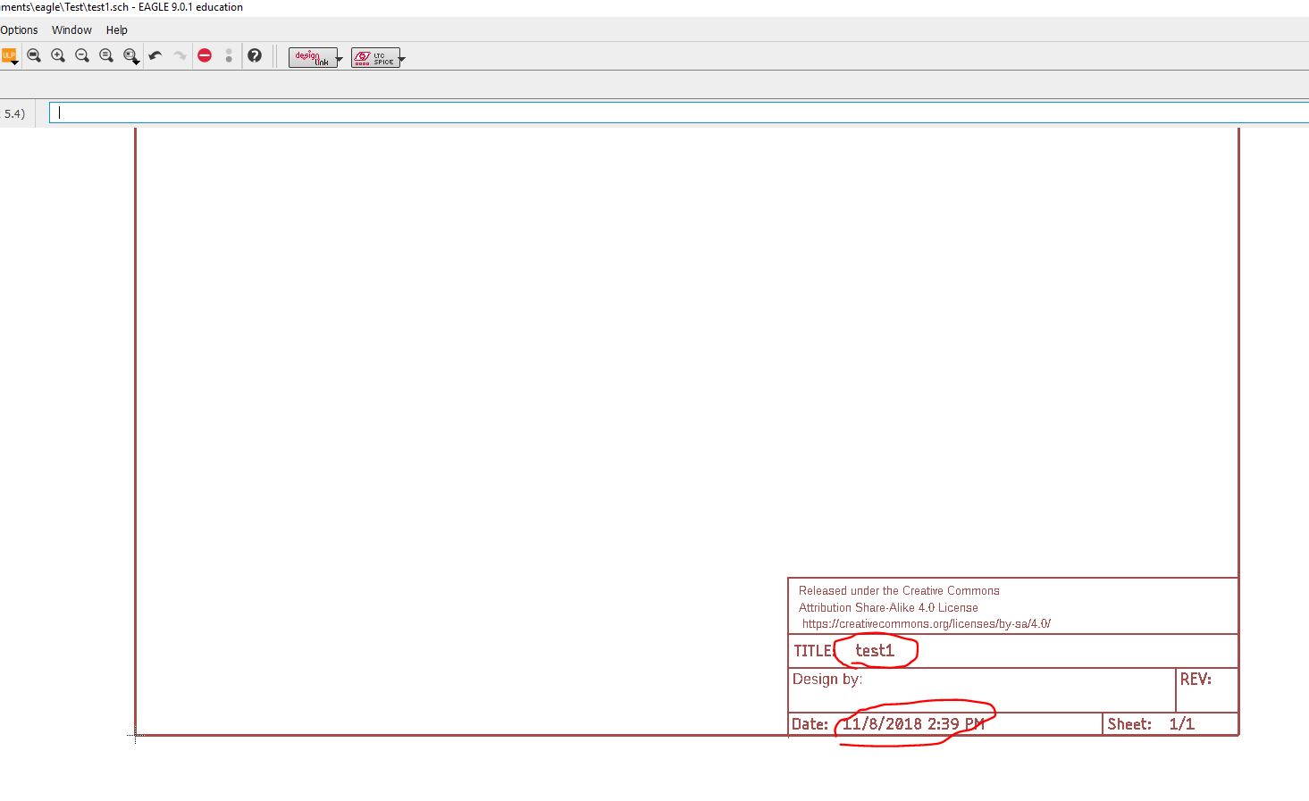
After selecting the part you want to add, it’ll “glow” and start hovering around following your mouse cursor. To place the part, left-click (once!). Let’s place the frame so its bottom-left corner runs right over our origin (the small dotted cross, in a static spot on the schematic). You can find the title and the date of the schematic is showing at the right bottom corner.
After placing a part, the add tool will assume you want to add another – a new frame should start following your cursor. To get out of the add-mode either hit escape (ESC) twice or just select a different tool.
Step 2: Save (And Save Often)
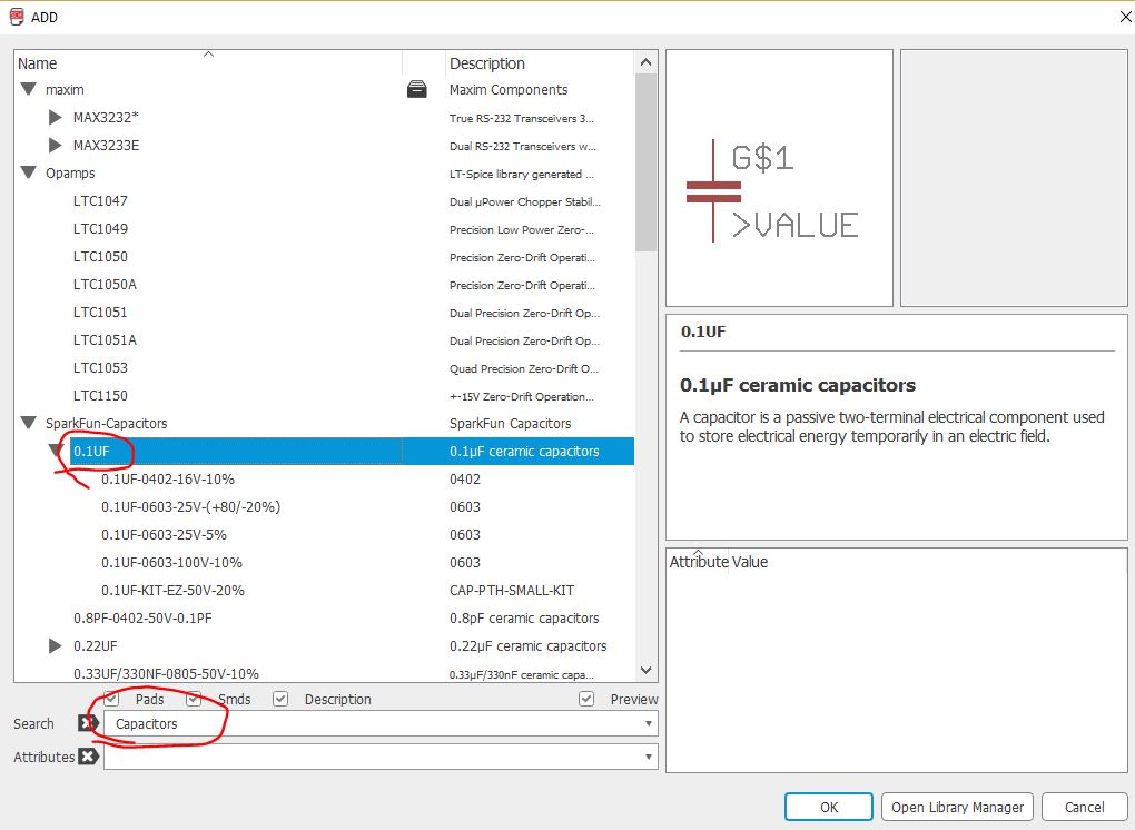
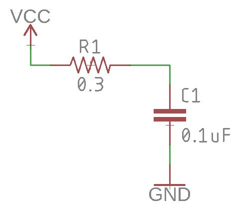
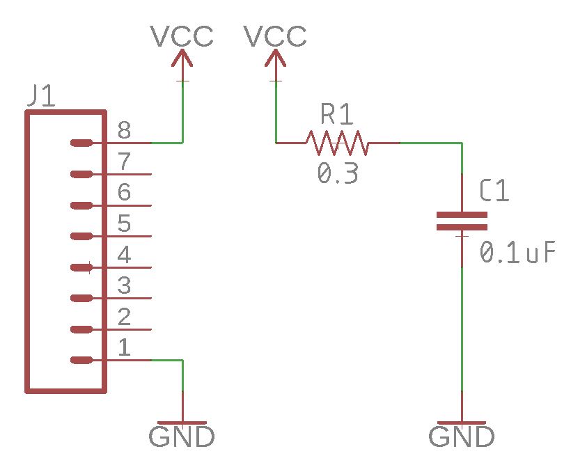
Step 3: Adding the Power Input Next we’ll add four different parts all devoted to our voltage supply input. Use the add tool for these parts:
Next we’ll add four different parts all devoted to our voltage supply input. Use the add tool for these parts:.
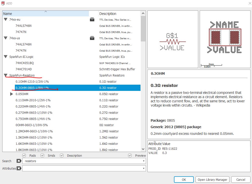
1. Capacitors
2. Resistor
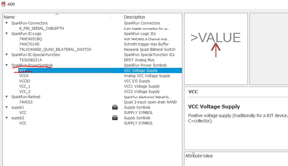
3. VCC
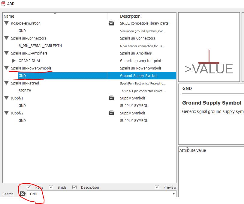
4. GND
All the components have a '+' in or beside the symbol, use your mouse, left click the cross and hold it then you can move it around.
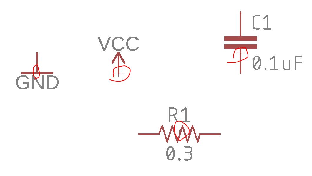
When you want to delete the component, you must single left click the cross to select the component, and press the 'delete' button on the keyboard.
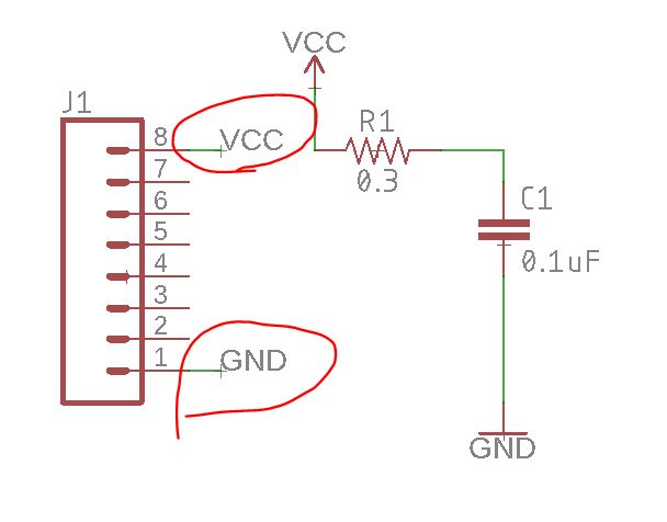
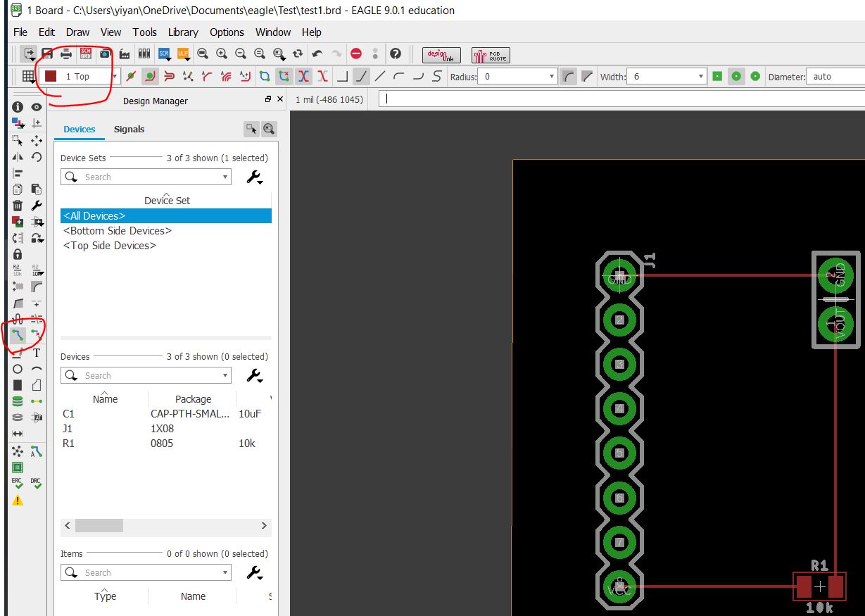
Let's make an RC circuit out of these components. Make sure you don't connect VCC to GND, this will short the power supply.
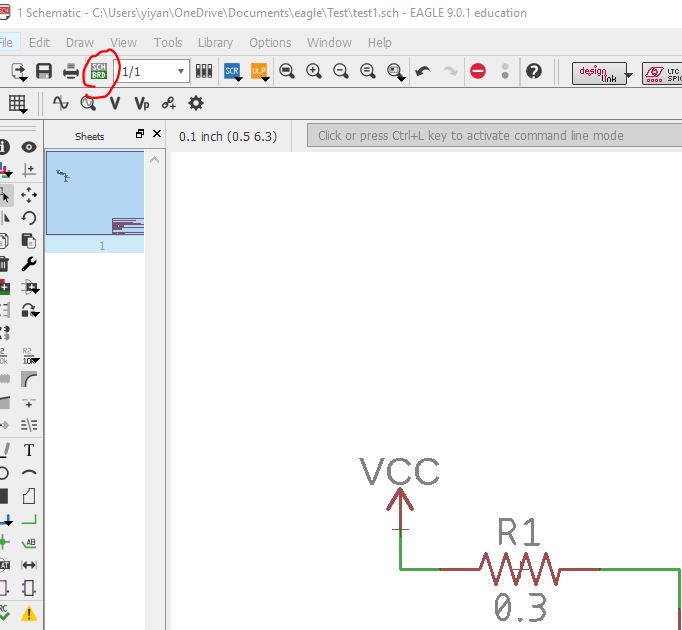
Click the schematic to board 'SCH BRD' button, Eagle will ask you if you want to create a new brd view since you don't have one so far. Click YES/.
You'll see the brd view as follows, and the layout of the components are outside of the layout window:
You have noticed that there is no layout view for VCC and GND, but only a single resitor and a single capacitor.
The reason is the VCC and GND symbols in the schematic view doesn't represent a REAL component but only an electrical node.
So we need to go back to the schematic view to put connectors, which are real components, for VCC and GND.
Search for '*CONN_08*:
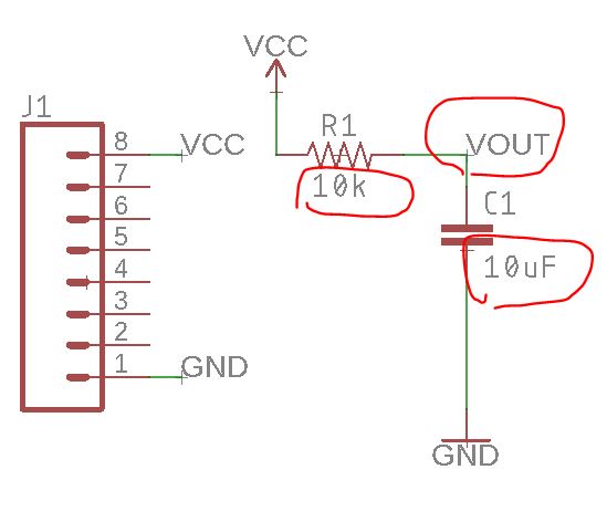
Now, I connect VCC and GND to the header, and keep the VCC and GND symbol at in the RC circuit. This will let Eagle know that all the voltage nodes with VCC and GND connected to them are electrically connected (the same voltage node).
Now, click the SCH BRD button on the top, you will see this:
The dashed wire (airwires) highlighted there indicates electrical connection and does not mean you have a PHYSICAL copper wire there. You need to place the components on the layout area and Route all the traces with copper wires to complete this.
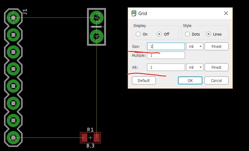
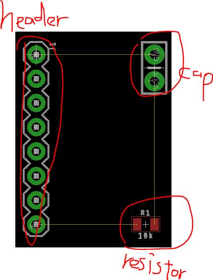
Now, let's move the components in the BRD view to the black area.
You can change the Grid settings to have the components aligned well:
To name the same voltage node, you do not have to connect them with the wires. You can also right click and give the node the same name. The nodes with the same names will be connected in the physical layout.
Right click the resistor, select 'value', change it to the desired value. This will only change the label of this component, resistors with different values can be in the same layout (package). The resistor package we use here is SMT 0805, which is one of many standard SMT packages. Change the falue of the resitor and the capacitor, also label the node between the resistor and the capacitor as 'VOUT'.
Now switch to the BRD view, you will see the labels have been changed.
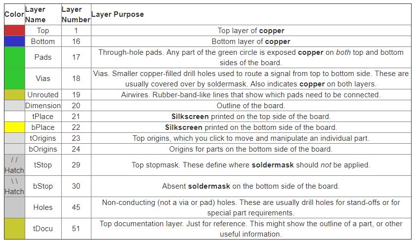
Layers Overview
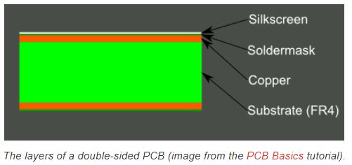
PCB composition is all about layering one material over another. The thickest, middle part of the board is a insulating substrate (usually FR4). On either side of that is a thin layer of copper, where our electric signals pass through. To insulate and protect the copper layers, we cover them with a thin layer of lacquer-like soldermask, which is what gives the PCB color (green, red, blue, etc.). Finally, to top it all off, we add a layer of ink-like silkscreen, which can add text and logos to the PCB.
EAGLE’s Layers The EAGLE board designer has layers just like an actual PCB, and they overlap too. We use a palette of colors to represent the different layers. Here are the layers you’ll be working with in the board designer:
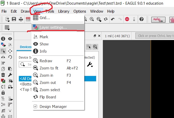
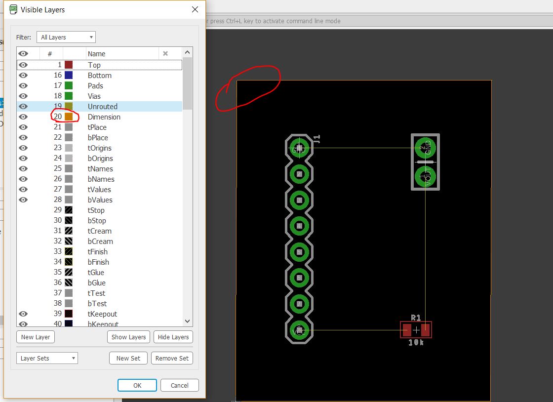
Go to View - Layer settings, you can turn on or off layers by selecting or deselecting it.
Selecting From Overlapping Objects Here’s one last tip before we get to laying our board out. This is an interface trick that trips a lot of people up. Since the board view is entirely two-dimensional, and different layers are bound to overlap, sometimes you have to do some finagling to select an object when there are others on top of it. Normally, you use the mouse’s left-click to select an object (whether it’s a trace, via, part, etc.), but when there are two parts overlapping exactly where you’re clicking, EAGLE doesn’t know which one you want to pick up. In cases like that, EAGLE will pick one of the two overlapping objects, and ask if that’s the one you want. If it is, you have to left-click again to confirm. If you were trying to grab one of the other overlapping objects, right-click to cycle to the next part. EAGLE’s status box, in the very bottom-left of the window, provides some helpful information when you’re trying to select a part.
We only have 3 components, the board can be very tiny. Change the Dimension layer's outline to fit to the three components. The Dimension layer is in the bronze color. If you check this color in the BRD window and the 'Visible Layers' window, you will see color is consistent.
Routing the Board Routing is the most fun part of this entire process. It’s like solving a puzzle! Our job will be turning each of those gold airwires into top or bottom copper traces. At the same time, you also have to make sure not to overlap two different signals.
Layer: On a 2-layer board like this, you’ll have to choose whether you want to start routing on the top (1) or bottom (16) layer.
Bend Style: Usually you’ll want to use 45° angles for your routes (wire bend styles 1 and 3), but it can be fun to make loopy traces too.
Width: This defines how wide your copper will be. Usually 0.01" is a good default size. You shouldn’t go any smaller than 0.007" (or you’ll probably end up paying extra). Wider traces can allow for more current to safely pass through. If you need to supply 1A through a trace, it’d need to be much wider (to find out how much, exactly, use a trace width calculator).
Via Options: You can also set a few via characteristics here. The shape, diameter, and drill can be set, but usually the defaults (round, auto, and 0.02" respectively) are perfect.
With those all set, you start a route by left-clicking on a pin where a airwire terminates. The airwire, and connected pins will “glow”, and a red or blue line will start on the pin. You finish the trace by left-clicking again on top of the other pin the airwire connects to. Between the pins, you can left-click as much as you need to “glue” a trace down.
With those all set, you start a route by left-clicking on a pin where a airwire terminates. The airwire, and connected pins will “glow”, and a red or blue line will start on the pin. You finish the trace by left-clicking again on top of the other pin the airwire connects to. Between the pins, you can left-click as much as you need to “glue” a trace down.
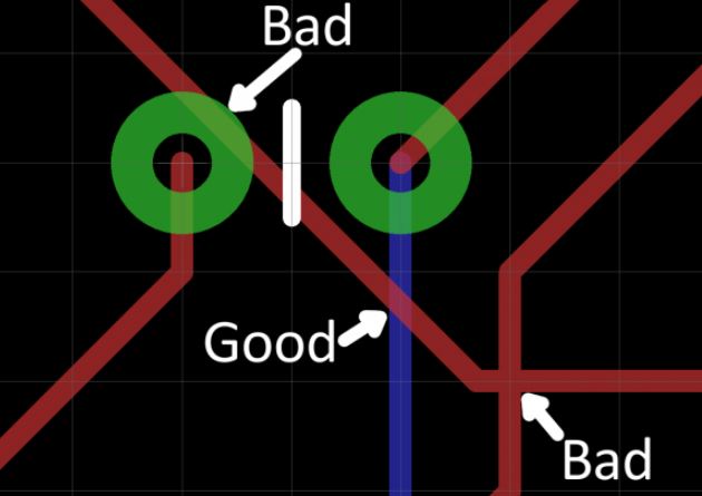
If traces do cross each other, make sure they do so on opposite sides of the board. It’s perfectly acceptable for a trace on the top side to intersect with one on the bottom. That’s why there are two layers! If you need more precise control over your routes, you can hold down the ALT key on your keyboard to access the alternate grid.
Placing Vias
Vias are really tiny drill holes that are filled with copper. We use them mid-route to move a trace from one side of the board to the other. To place a via mid-route, first left-click in the black ether between pins to “glue” your trace down. Then you can either change the layer manually in the options bar up top, or click your middle mouse button to swap sides. And continue routing to your destination. EAGLE will automatically add a via for you.

You can also place 'vias' manually. 'vias' are through holes.
Ripping Up Traces
Much like the WIRE tool isn’t actually used to make wires, the DELETE tool can’t actually be used to delete traces. If you need to go back and re-work a route, use the RIPUP tool – – to remove traces. This tool turns routed traces back into airwires. You can also use UNDO and REDO to back/forward-track.
Or Use the Autorouter (Cheater!)
If you’re short on time, or having trouble solving the routing puzzle, you can try loading up EAGLE’s Autorouter
Checking for Errors
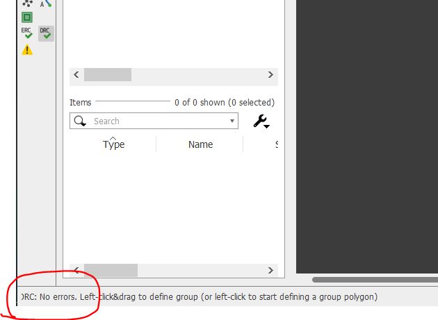
Before we package the design up and send it off to the fabrication house, there are a few tools we can use to check our design for errors. Ratsnest – Nothing To Do! The first check is to make sure you’ve actually routed all of the nets in your schematic. To do this, hit the RATSNEST icon – – and then immediately check the bottom left status box. If you’ve routed everything, it should say “Ratsnest: Nothing to do!”
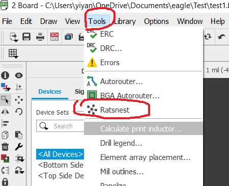
As denoted by the exclamation mark, having “nothing to do” is very exciting. It means you’ve made every route required. If ratsnest says you have “N airwires” left to route, double check your board for any floating golden lines and route them up. If you’ve looked all over, and can’t find the suspect airwire, try turning off every layer except 19 Unrouted.
Design Rule Check Once you’re done routing there’s just one more check to be made: the design rule check (DRC).
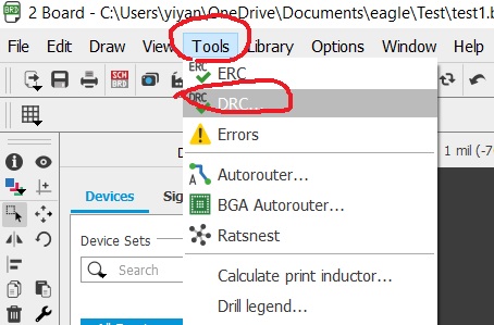
The results of the DRC check can be found at the bottom of the page:
Adding Copper
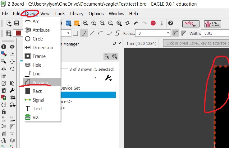
Pours Copper pours are usually a great addition to a board. They look professional and they actually have a good reason for existing. Not to mention they make routing much easier. Usually, when you’re adding a copper pour it’s for the ground signal. So let’s add some ground pours to the design.
Start by selecting the POLYGON tool. Select the top copper (1) layer. Also adjust the Isolate setting which defines how much clearance the ground pour gives other signals, 0.012" for this is usually good. Change 'width' to be 0.01, change spacing to be 0.05.
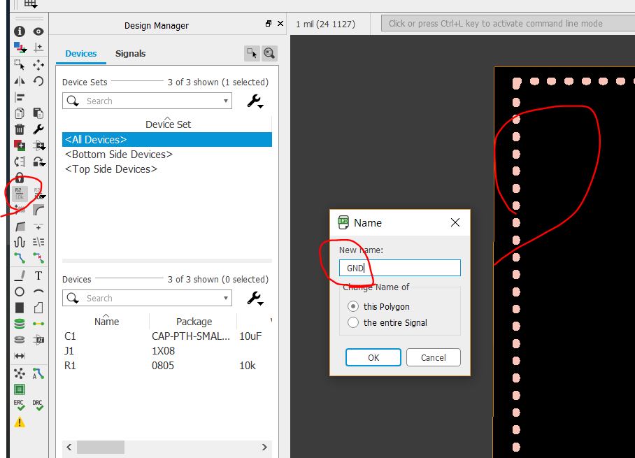
Right click the polygon and name it as GND. This works just like naming nets on a schematic.
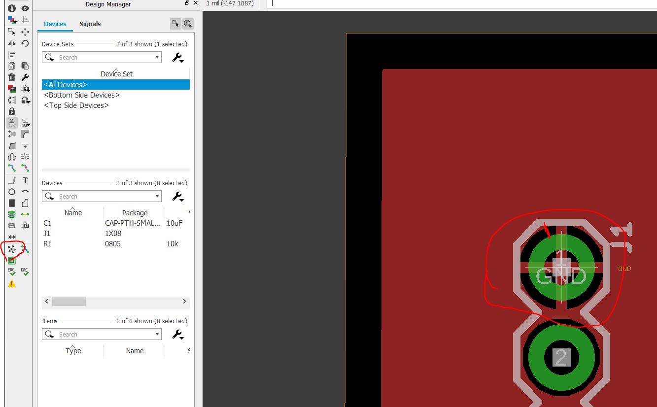
The last step is to hit ratsnest, to watch the glorious red pour fill just about the entire area of your board. You’ll probably hate me for telling you this now, but adding ground pours to your design at the very beginning (after placing parts, before routing) makes manual routing much easier. You can (and probably should) have ground pours on both sides of the board, so follow the same set of steps on the bottom layer.
The copper was poured to all the remaining space on the board, and connected to the GND pad.
Adding Silkscreen
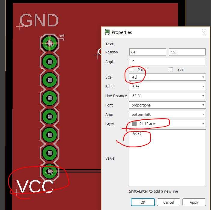
Although it has no real effect on the circuit your designing, silkscreen can be a critical part of the PCB design. You want it to look good, right? Some silkscreen – like part outlines – is automatically placed on the board because it’s a piece of the part. We can manually add other information, like labels, logos, and names. A variety of draw tools – wire, text, circle, arc, rectangle, and polygon – can be used to draw on the silkscreen layer (tPlace for top, bPlace for bottom). Have fun and explore with these tools. You could add labels for the headers, or values for the resistors, or even create a nifty logo.
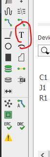
Select 'T' from the side bar.
Add texts. Right click the cross beside the text and change the size of the text.
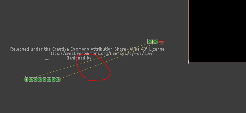
You can even draw a Fort Lewis College logo:

This final version of this project looks like this:
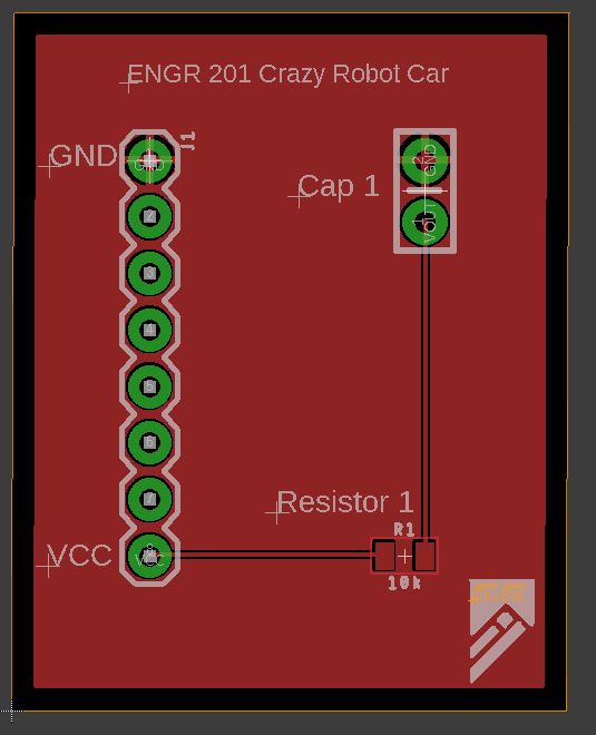
It is not a robot car circuit at all, it is just a simple RC circuit. You should be able to design a simple PCB now.
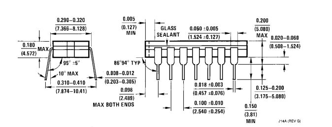
However, you cannot always find the package for the chips being used in your robot car circuit. In this case, you need to measure the dimension of the component and design the component library in eagle by yourself. The datasheet pdf of the components usually have the dimension information. For example: