Introduction:
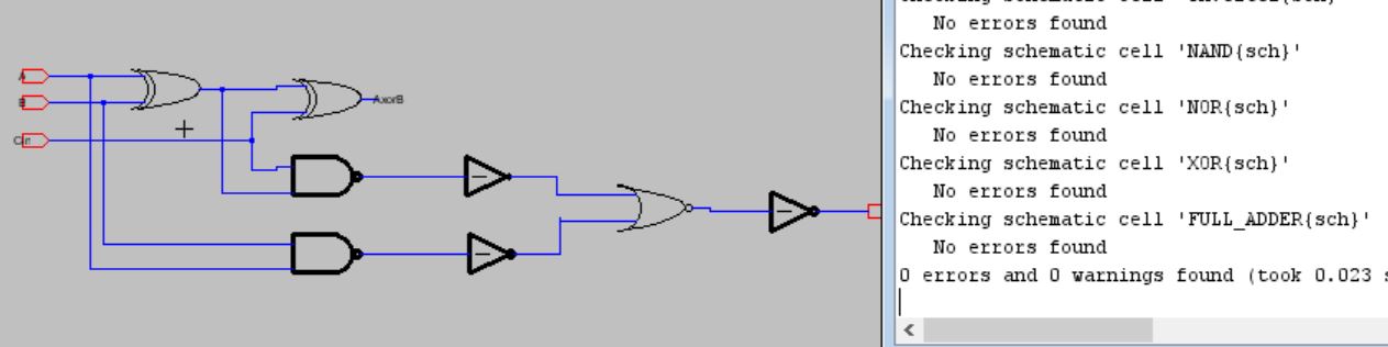
In this lab we created componets to build up to a full adder. These components included a NAND gate, NOR gate and XOR gate. Once all components were created I copied and pasted them into the main file of the full adder.
Task 1:
Building NAND gate
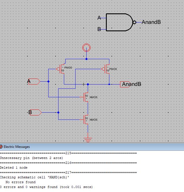
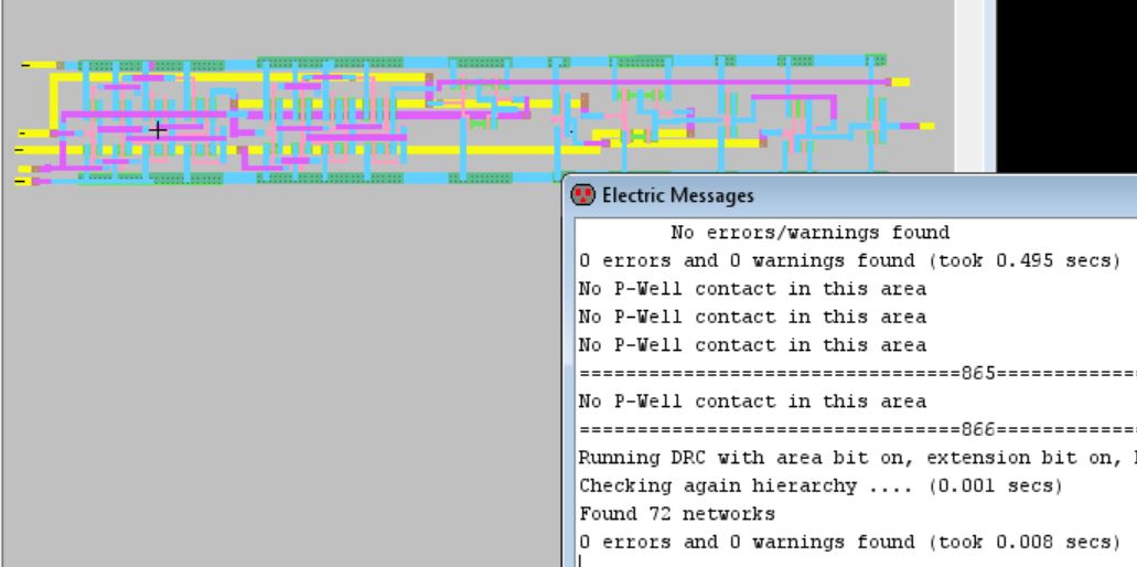
Figure 1: DRC clean of NAND gate
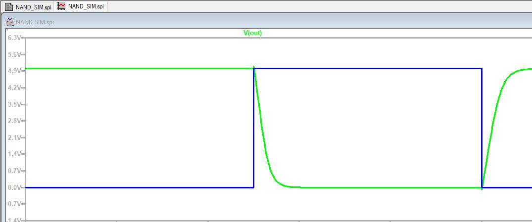
Figure 2: Simulation results of NAND gate
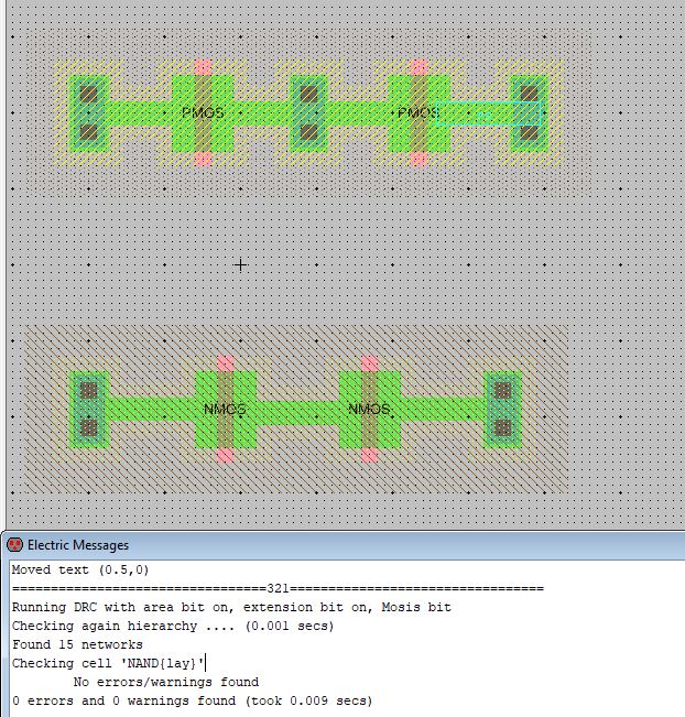
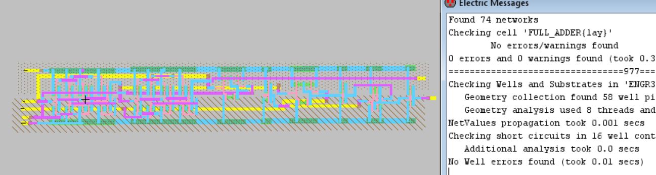
Figure 3: DRC clean of NAND gate, note that this was modified later to work better with full adder
Task 2:
Schematic and layout of NOR gate
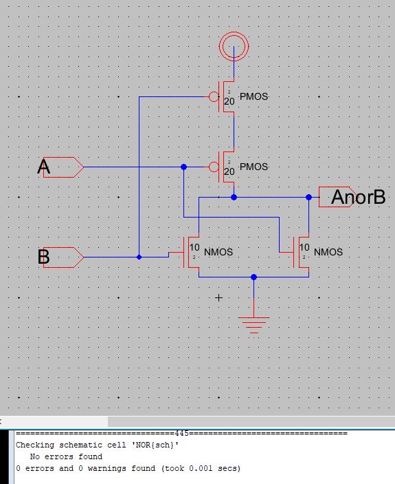
Figure 4: DRC clean NOR gate schematic
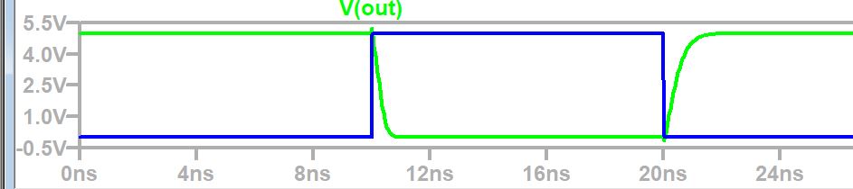
Figure 5: NOR simulation results
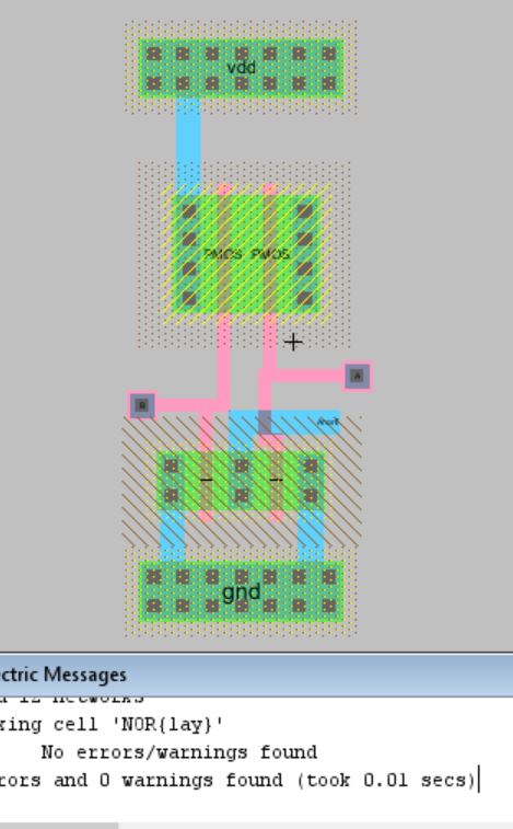
Figure 6: DRC clean of NOR gate layout
Important to note that the wells of this were later change to pass ERC checks, changes can be seen in the full adder.
Task 3:
Design and layout of XOR gate
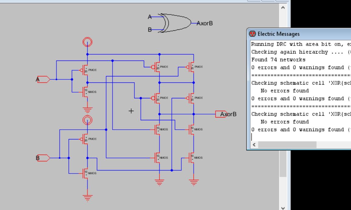
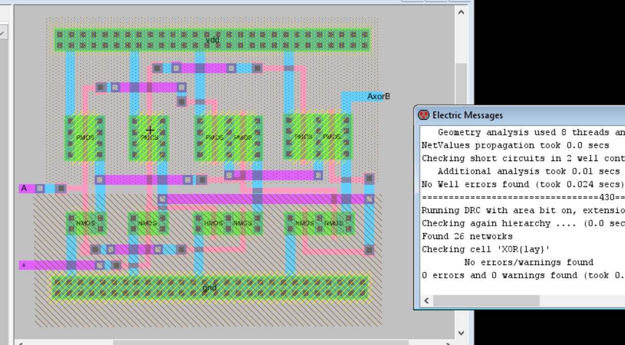
Figure 7: DRC clean of XOR gate
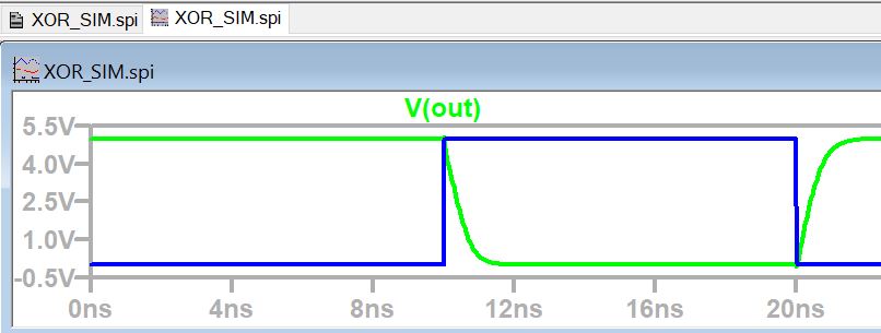
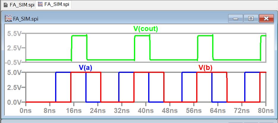
Figure 8: Simulation results for XOR gate, B pin is held high
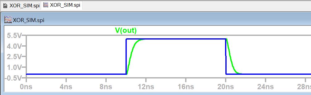
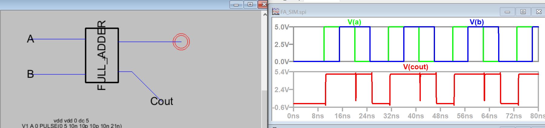
Figure 9: