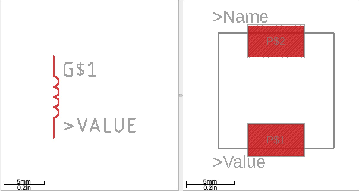
Figure 1: Symbol and Footprint of created inductor device.
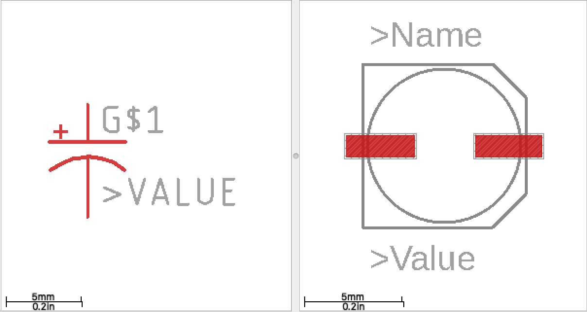
Figure 2: Symbol and Footprint of created capacitor device.
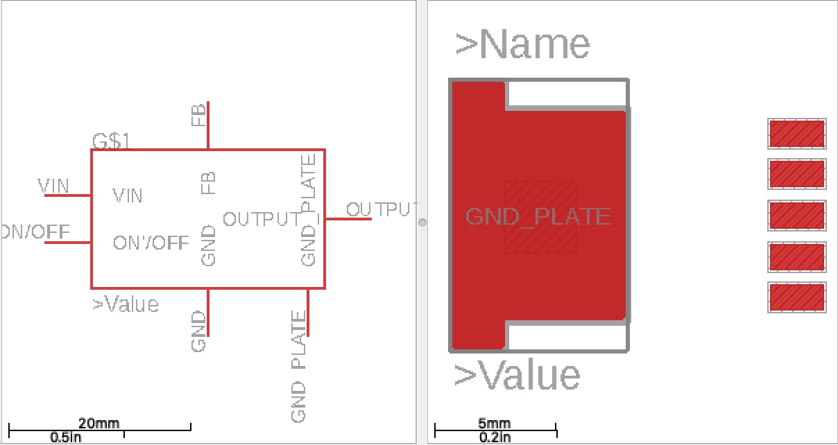
Figure 3: Symbol and Footprint of created LM2596 device.
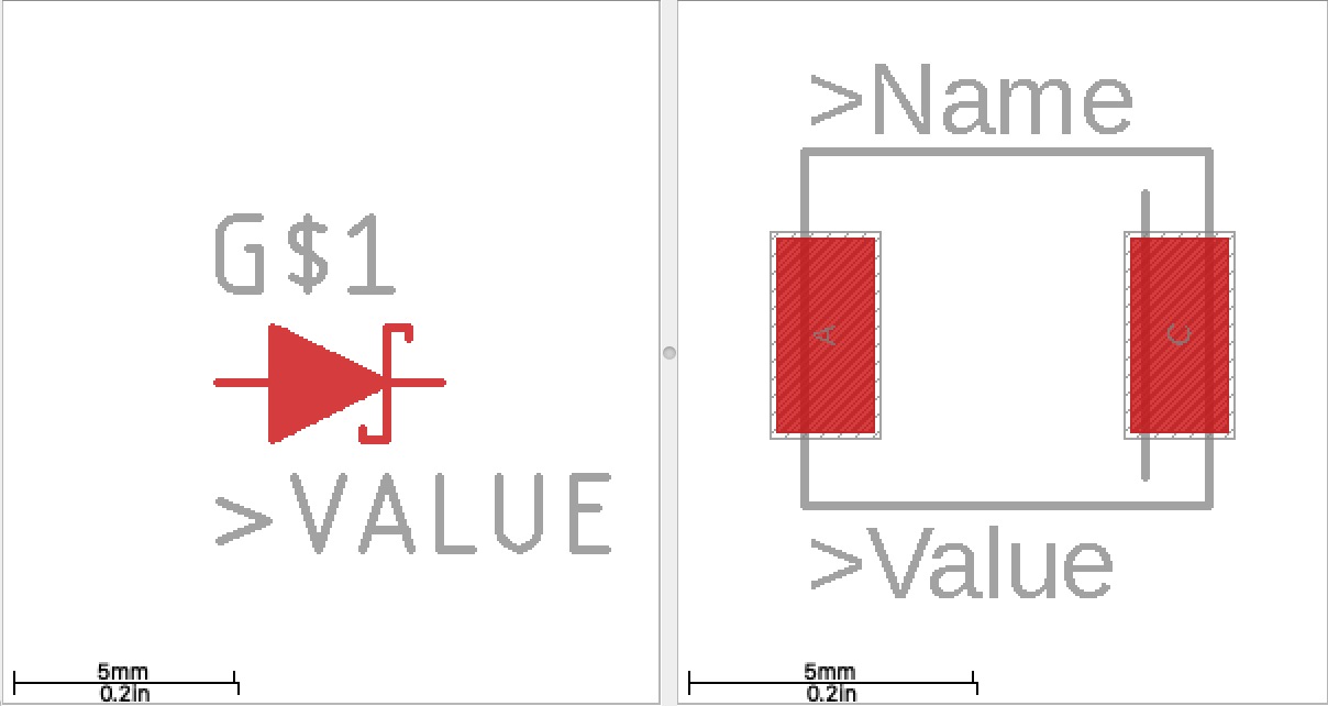
Figure 4: Symbol and Footprint of created SS34 Schottky Diode device.
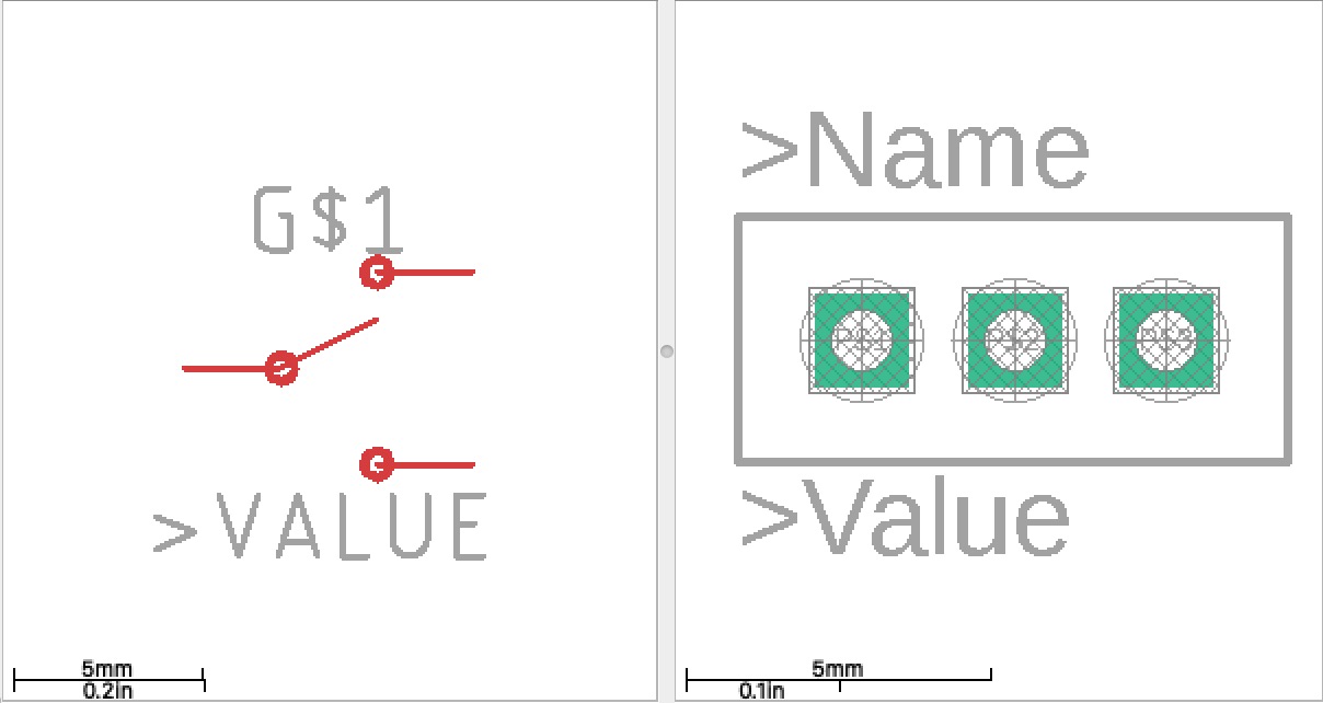
Figure 5. Symbol and Footprint of created switch.
Schematic Layouts In Eagle
Once we have the devices created we can use them and the devices in the SparkFun library to create the needed schematics. Once the final schematic is done an Electric Rule Check (ERC) check needs to be ran to make sure all nets are properly connected, check for conflicting outputs/inputs, and check if there are any open or overlapping pins and ports.
Once we have the devices created we can use them and the devices in the SparkFun library to create the needed schematics. Once the final schematic is done an Electric Rule Check (ERC) check needs to be ran to make sure all nets are properly connected, check for conflicting outputs/inputs, and check if there are any open or overlapping pins and ports.
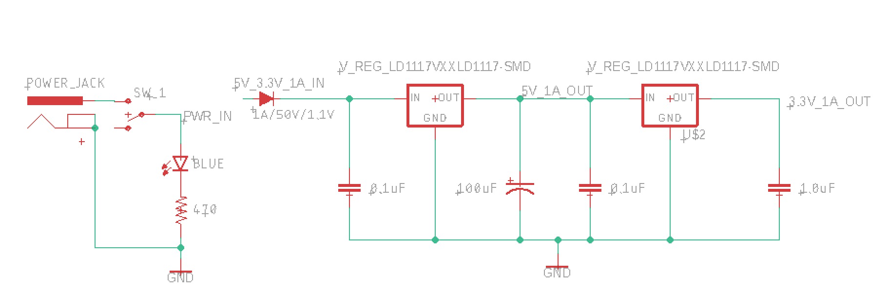
Figure 6: Schematic using SparkFun parts and homemade switch .
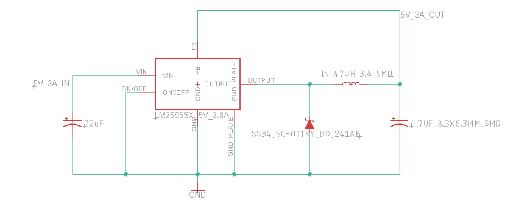
Figure 7: Schematic using homemade parts.
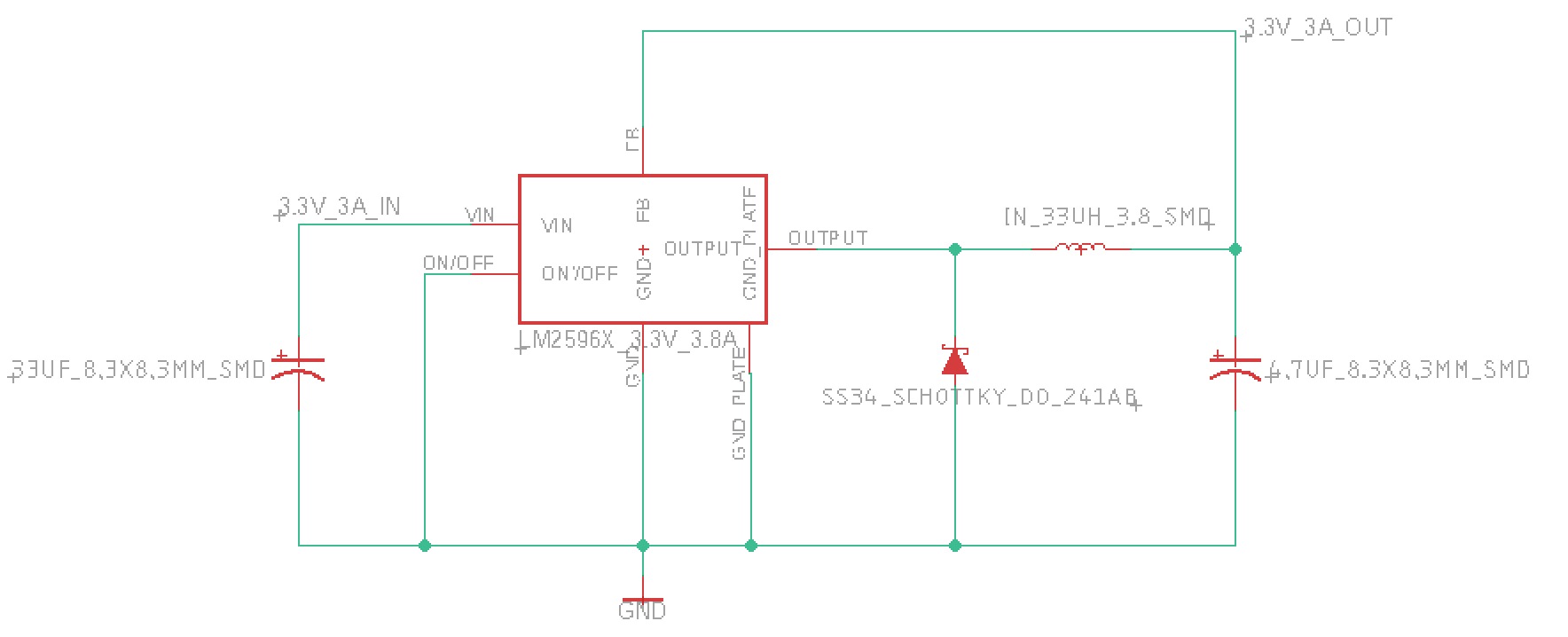
Figure 8: Schematic using homemade parts.
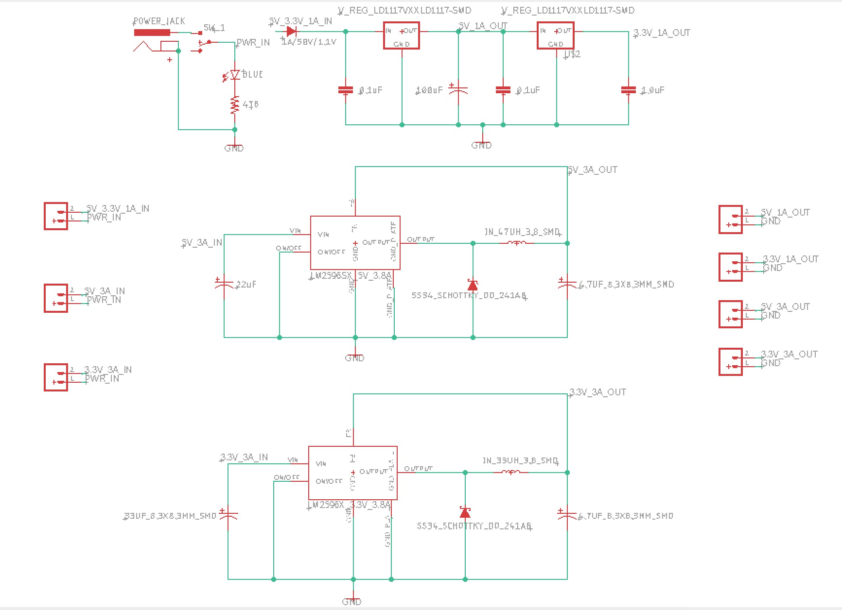
Figure 9: Final schematic layout.
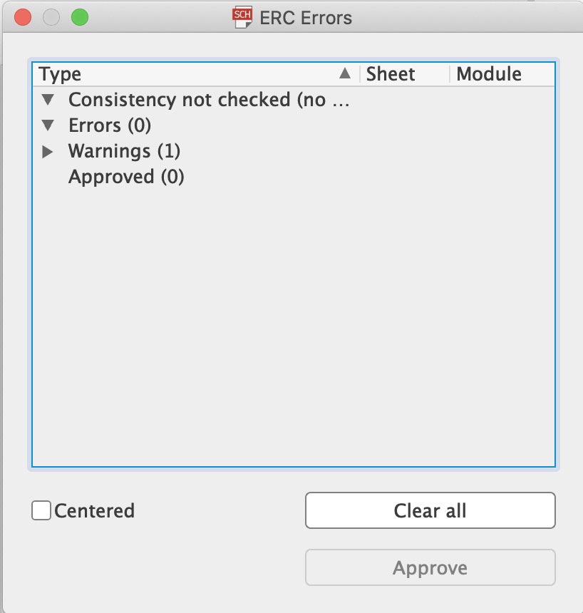
Figure 10: ERC check.
BRD (PCB) Layouts In Eagle
Once the schematic is all done, the schematic is used to create the BRD (PCB) view and the parts can be moved to your preference.
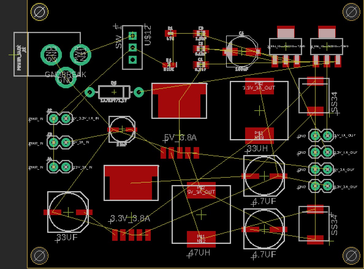
Figure 11: BRD (PCB Layout) before routing of Figure 9.
DRC Check
Once the layout is configured a Design Rule Check (DRC) check is needed to be ran to check if the PCB design abides by the manufacturing-specific constraints.
Once the layout is configured a Design Rule Check (DRC) check is needed to be ran to check if the PCB design abides by the manufacturing-specific constraints.
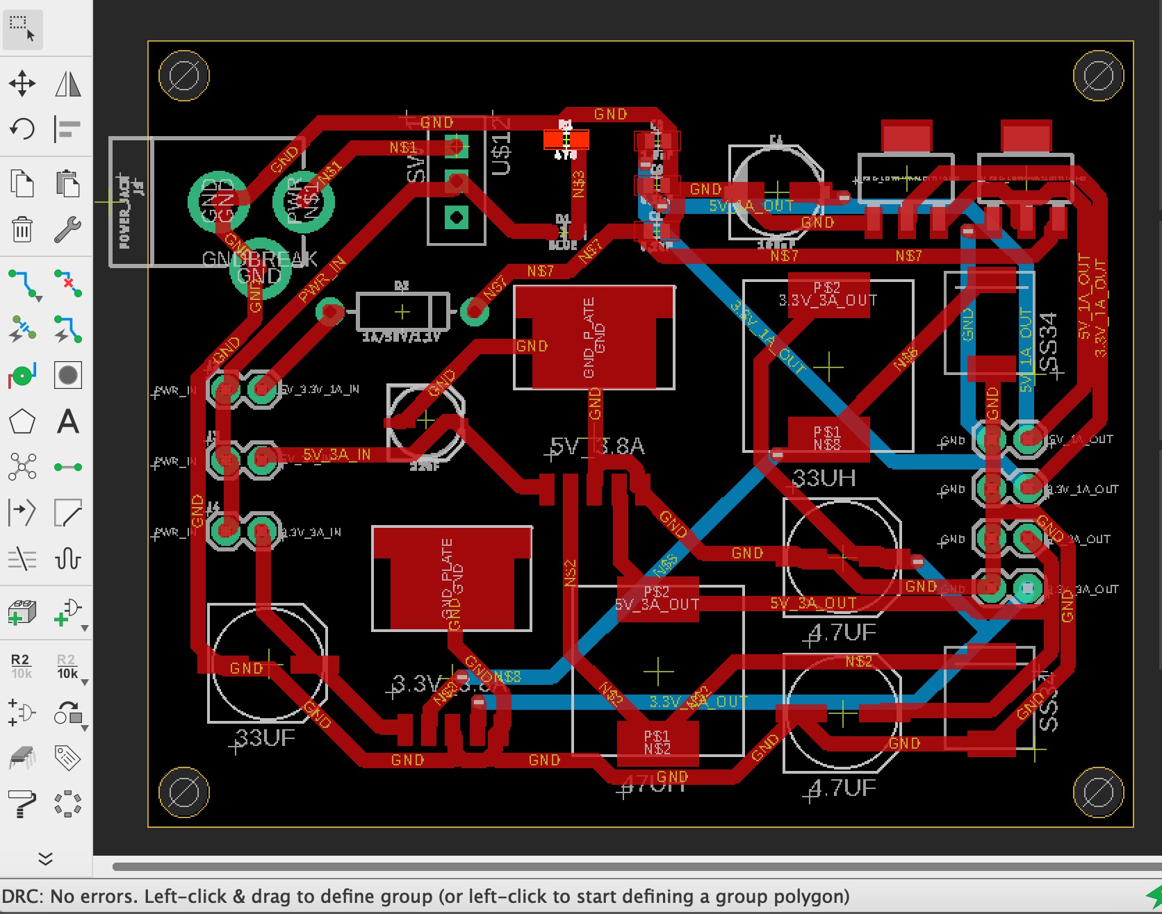
Figure 12: BRD (PCB Layout) with routing and DRC check.
Ratsnest Check
After the DRC check is ran, a Ratsnest check needs to be ran just to make sure that all the nest are actually routed.
After the DRC check is ran, a Ratsnest check needs to be ran just to make sure that all the nest are actually routed.

Figure 13: BRD (PCB Layout) with routing and Ratsnest check.
Copper Pour For PCB
Once all the checks have been completed, copper can finally be poured on the top and bottom of the PCB.
Once all the checks have been completed, copper can finally be poured on the top and bottom of the PCB.
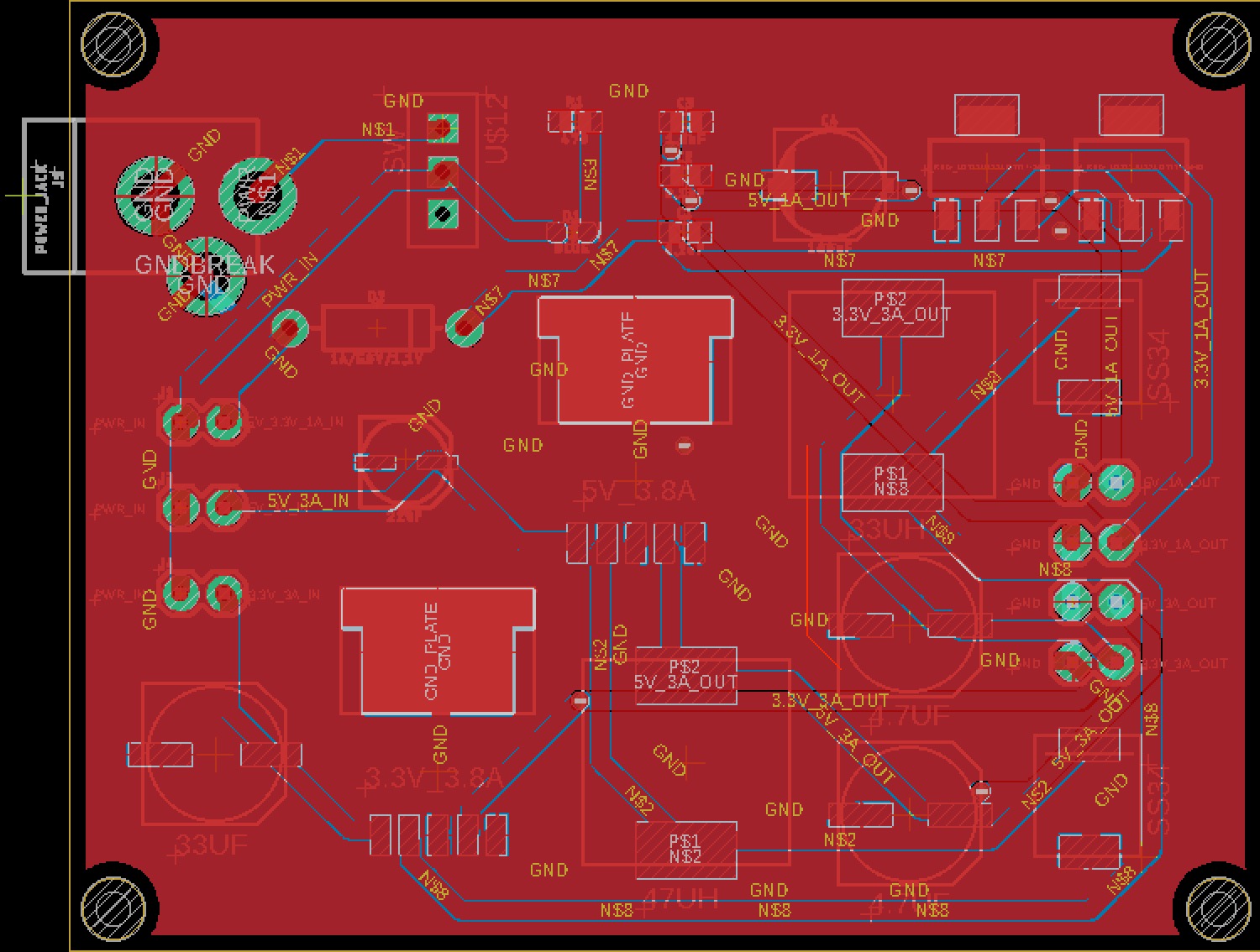
Figure 14: BRD view with the copper poured on.
PCB View Results
Now the PCB can be prepared for manufacturing by getting the Gerber Files associated with your PCB and uploading them to a PCB View to check to see is all the layers are visible and to your liking. Finally, if everything checks out the Gerber Files can be submitted to PCBWay to be fabricated.
Now the PCB can be prepared for manufacturing by getting the Gerber Files associated with your PCB and uploading them to a PCB View to check to see is all the layers are visible and to your liking. Finally, if everything checks out the Gerber Files can be submitted to PCBWay to be fabricated.
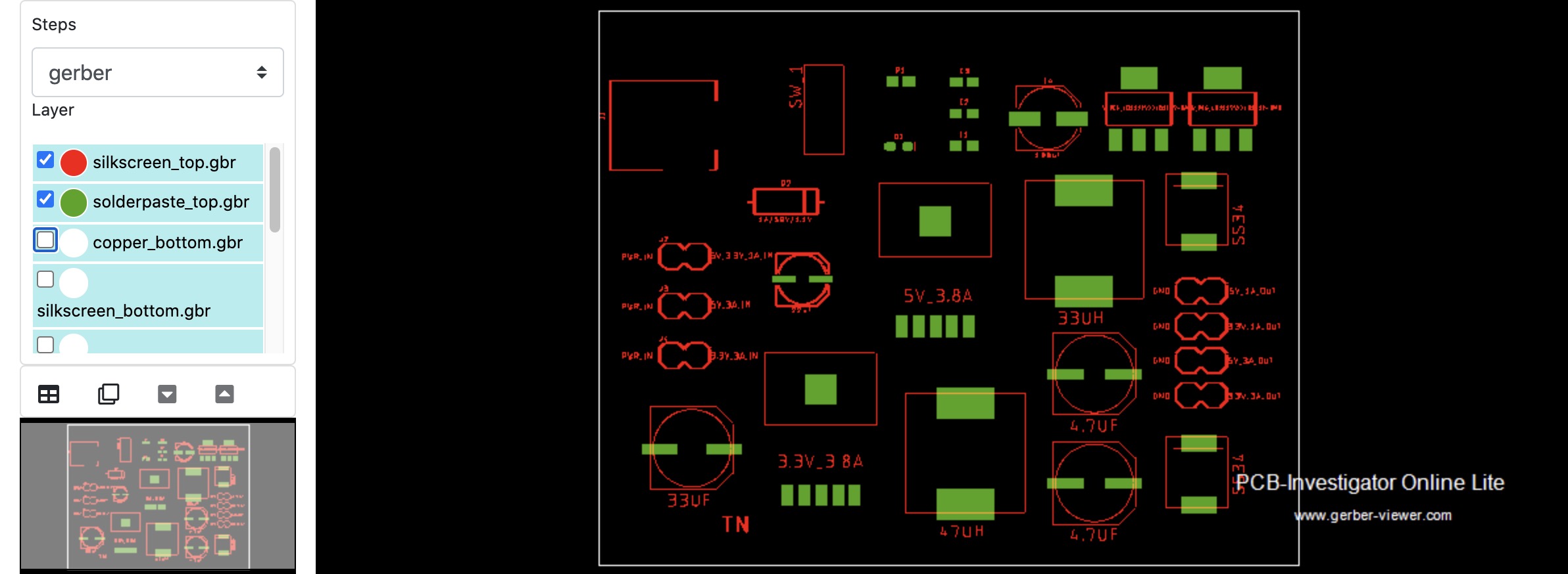
Figure 15: PCB Investigator showing the top silkscreen (tPlace, tNames) and top solderpaste (tCream).
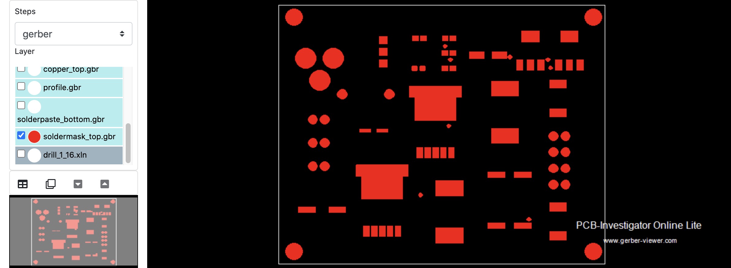
Figure 16: PCB Investigator showing the top soldermask (tStop).
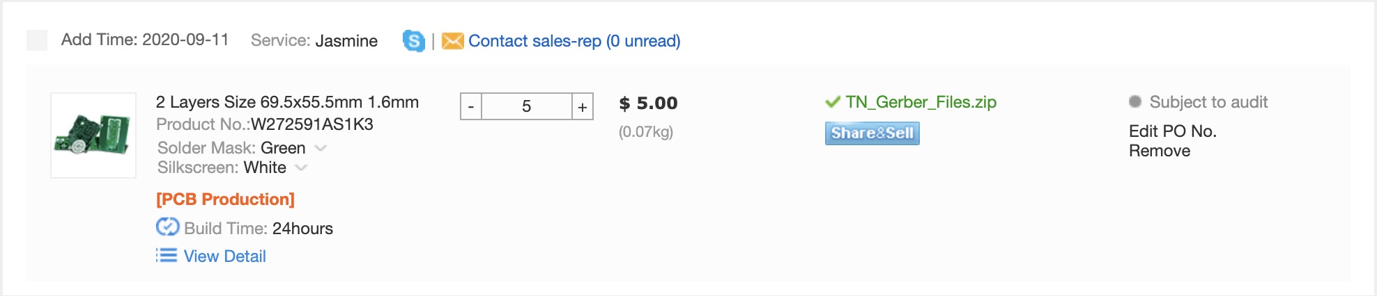
Figure 17. Uploaded gerber files to PCBWay.
Fabricated PCB
After a couple weeks we were able to get the fabricated PCB boards from PCBWay, which we received 10 boards, as shown in Figure 18. We were given the parts, which we had to solder onto the PCB board as shown in Figure 19. Once everything was soldered onto the board, it was time to test the board to see if it gave the desired output as shown in Figures 20-24.
After a couple weeks we were able to get the fabricated PCB boards from PCBWay, which we received 10 boards, as shown in Figure 18. We were given the parts, which we had to solder onto the PCB board as shown in Figure 19. Once everything was soldered onto the board, it was time to test the board to see if it gave the desired output as shown in Figures 20-24.
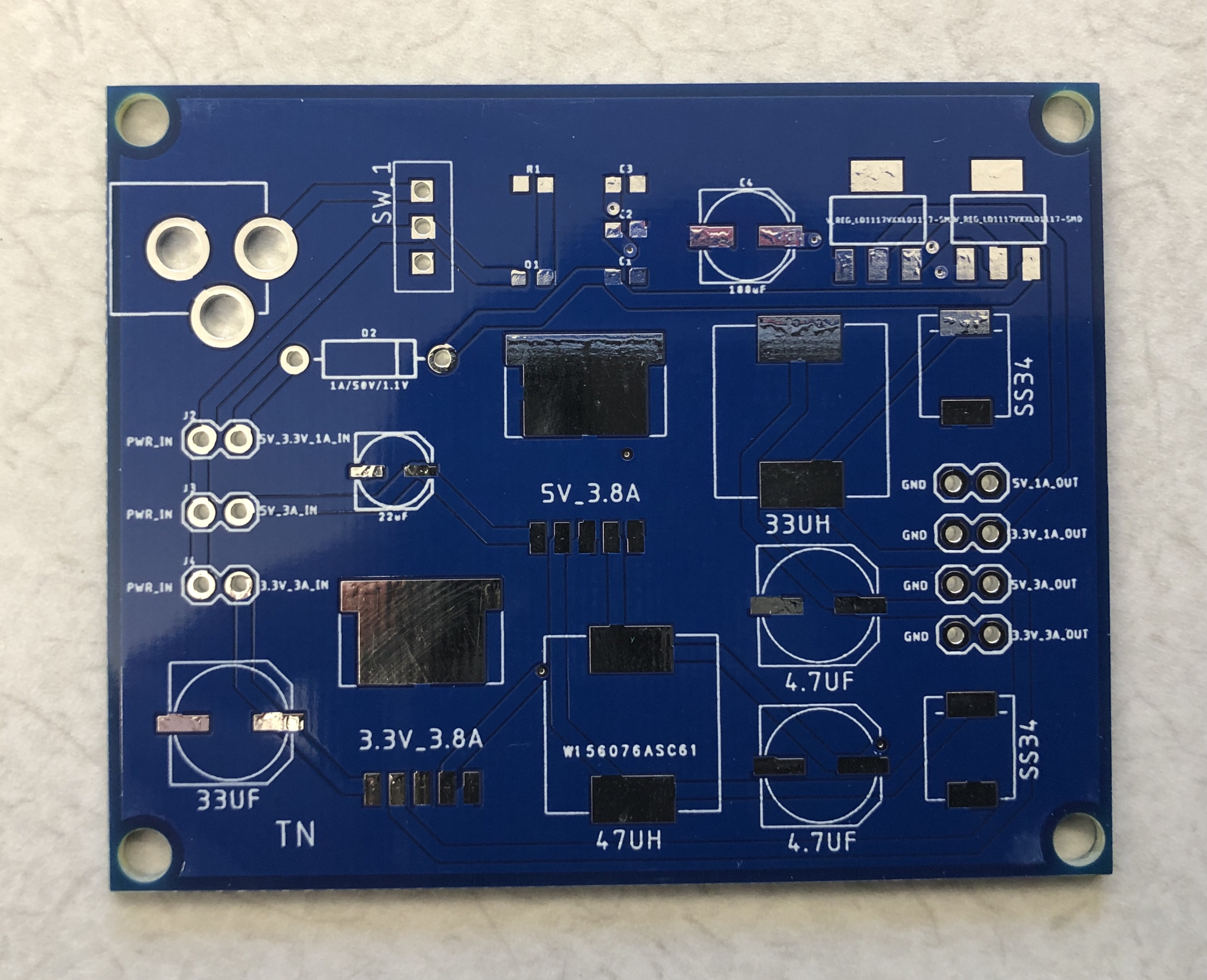
Figure 18. Bare PCB with no components on.
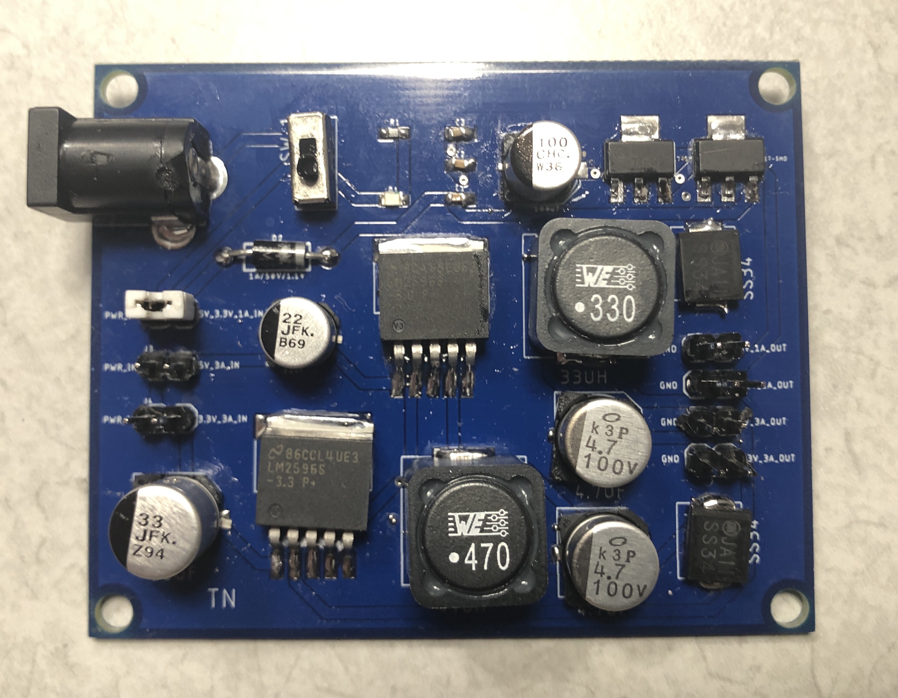
Figure 19. PCB Board with soldered parts.
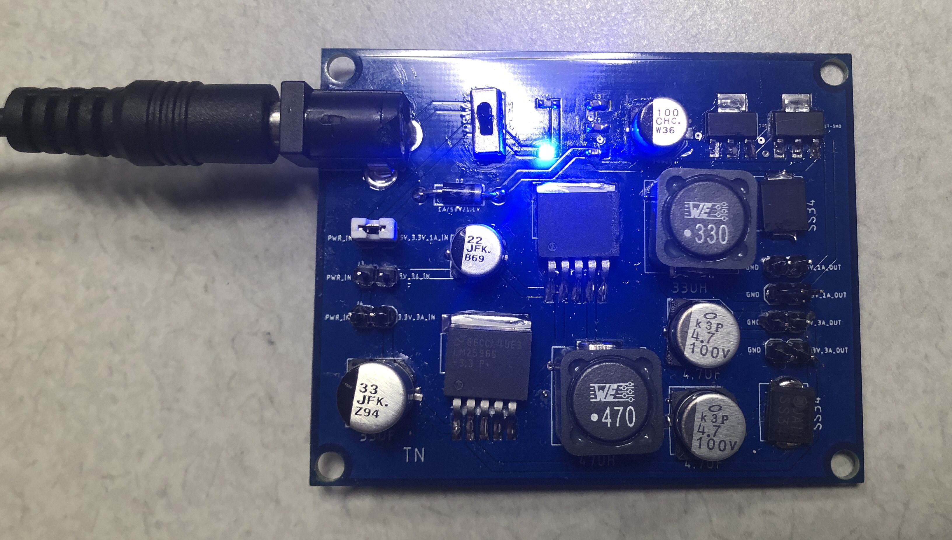
Figure 20. PCB board powered on.
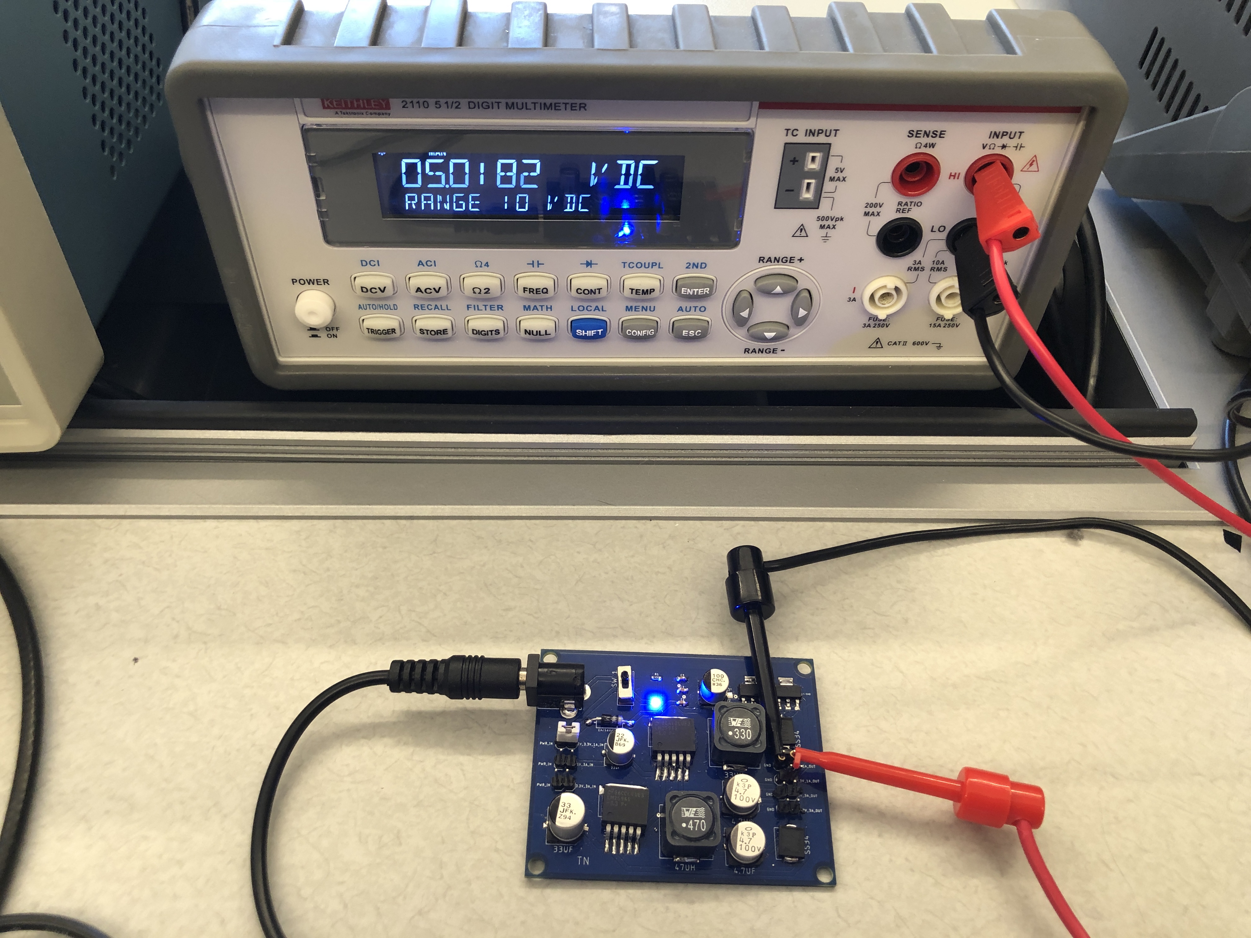
Figure 21. Checking voltage of 5V 1A output pin.
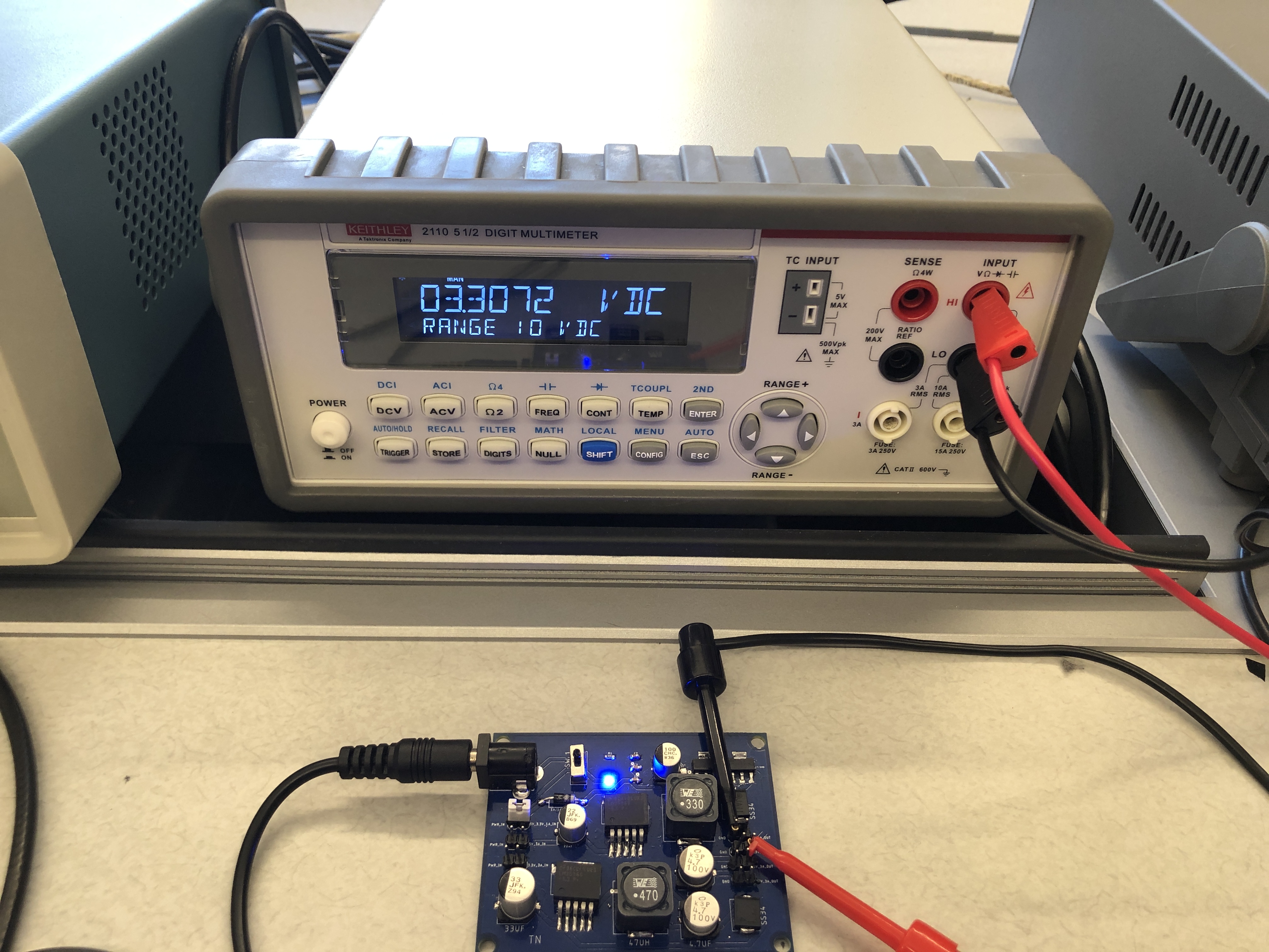
Figure 22. Checking voltage of 3.3V 1A output pin.
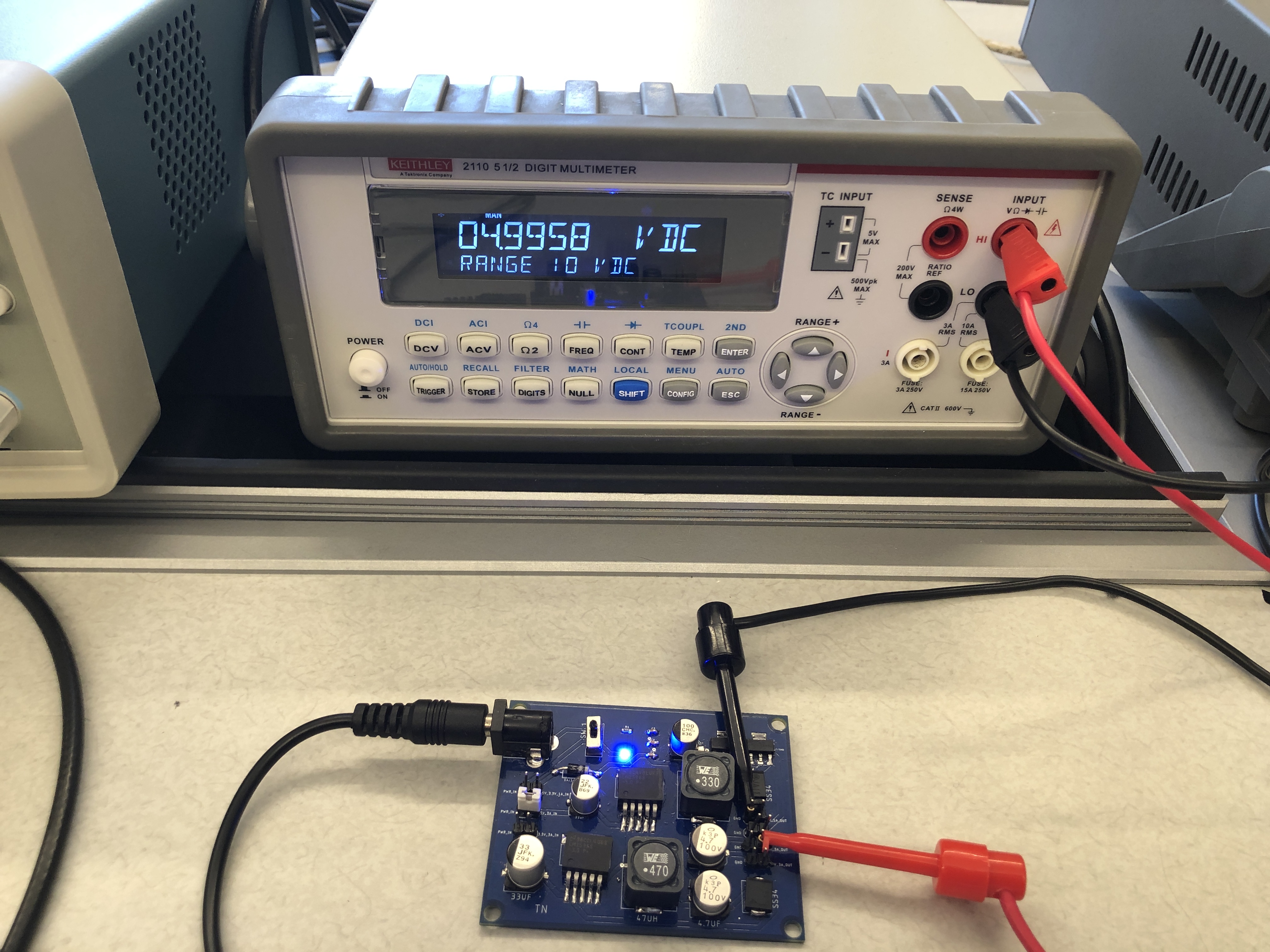
Figure 23. Checking voltage of 5V 3A output pin.
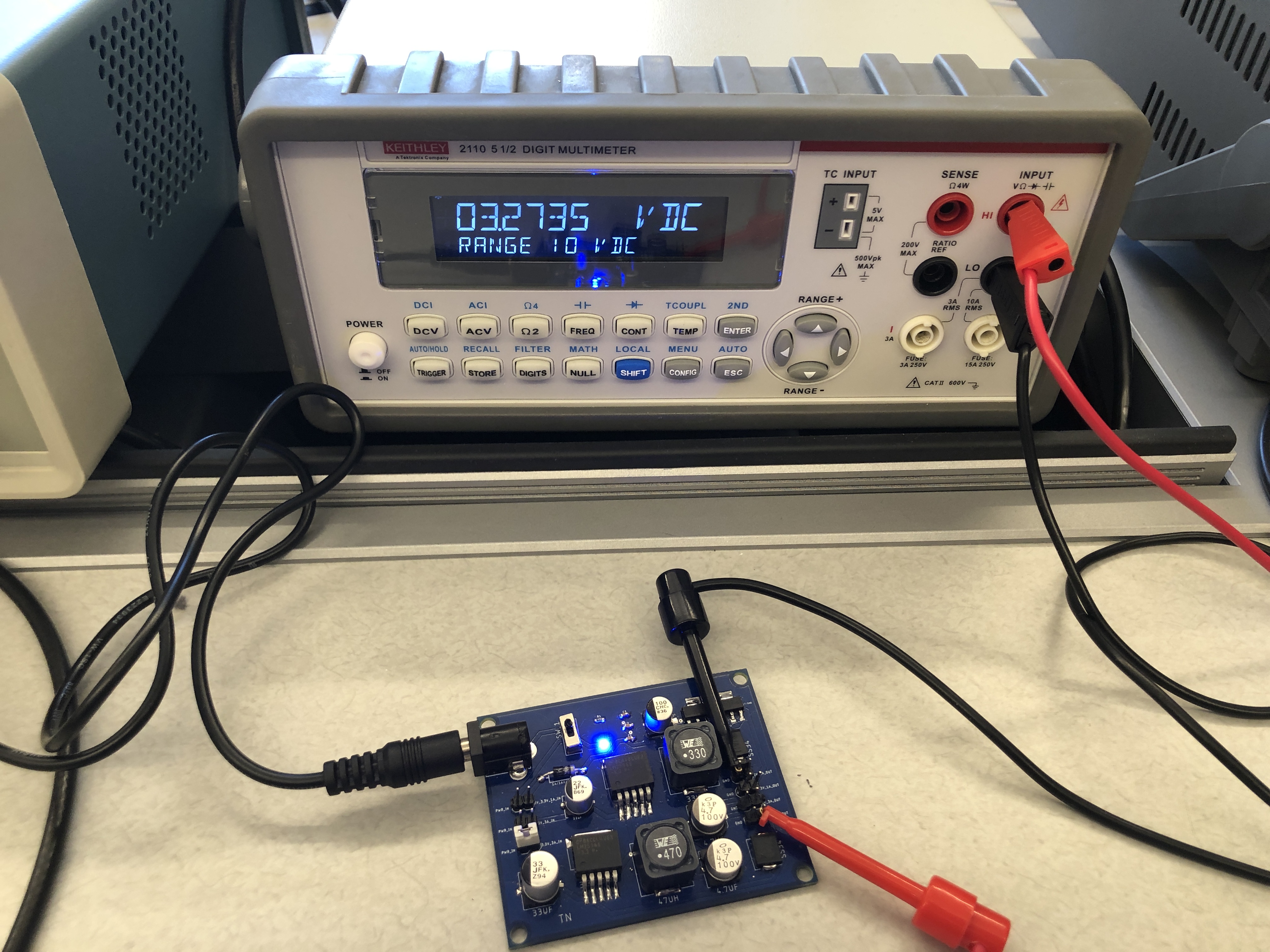
Figure 24. Checking voltage of 3.3V 3A output pin.
Discussion
..........................