ENGR 338 2021 Spring
Lab 9: Design a Simple 8-bit ALU in ElectriVLSI
Taylor Nakai
tsnakai@fortlewis.edu
Introduction:
In
this lab, we used ElectriVLSI to build an 8-bit ALU (Arimetic Logic
Unit). For the 8-bit ALU we had to create a schematic, icon, and
layout. We were able to use the 8-bit MUX, 8-bit Inverter, 8-bit AND
gate, 8-bit OR gate, and 8-bit High-Speed MUX that we had previously
created to create the schematic and layout for the ALU. We tested the
ALU by conducting simulations using LTSpice.
Task 1:
In
task 1, we were given the task to design the logic circuit fo the ALU.
The 8-bit ALU would be able to perform AND, OR, ADD, and SUB
operations. In order to do so we needed to make sure that we had all of
the components needed to create the schematic. Since we created all the
needed schematics and icons in previous labs it was easy to create the
schematic and icon of the 8-bit ALU shown in Figure 1. In order to make
sure that the components were fuctioning correctly and the logic of the
ALU was correct, we ran simulations using LTSpice. The simulations ran
tested the AND, OR, ADD, and SUB functionalities as shown in Figure 2 -
5.
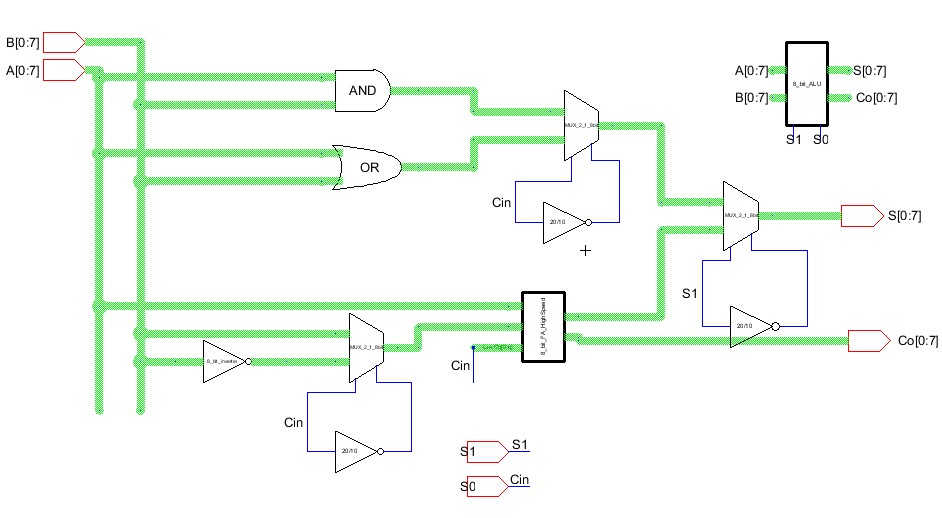
Figure 1. Schematic and icon of 8-bit ALU.
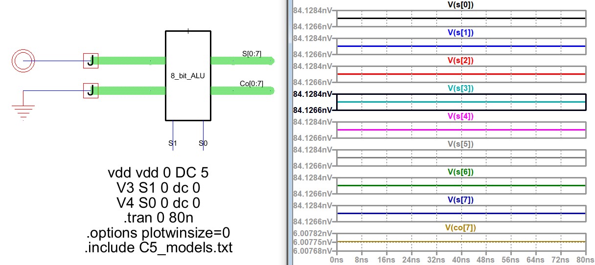
Figure 2. Simulation to verify AND gate by setting S1 and S0 to 0..
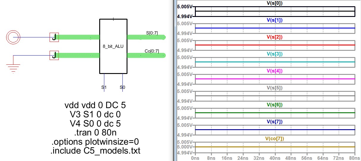
Figure 3. Simulation to verify the OR gate by setting S1 to 0 and S0 to 1.
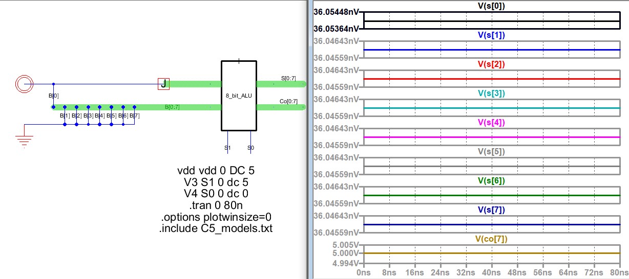
Figure 4. Simulation to verify the ADD operation and the result should be 0000 0000 with a Co of 1.
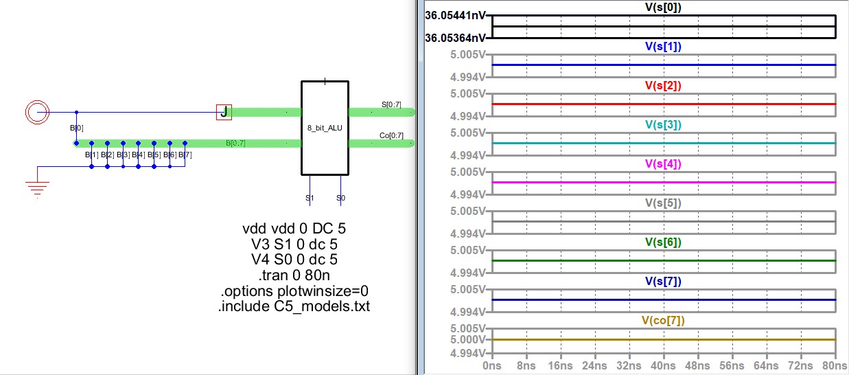
Figure 5. Simulation to verify the subtraction operation and the result should be 1111 1110 with a Co of 1.
Task 2:
In
task 2, we were given the task of building the layout of the ALU in
ElectriVLSI. Using the layout that we had created, shown in Figure 6,
we were able to create the layout. We had to create the layout of the
components that we did not have in our personal library. Once we had
all the layouts we were able to create the ALU's layout as shown in
Figure 7. To ensure that the schematic and layout match we ran a DRC
and NCC check to confirm that everthing matched as shown in Figure 8.
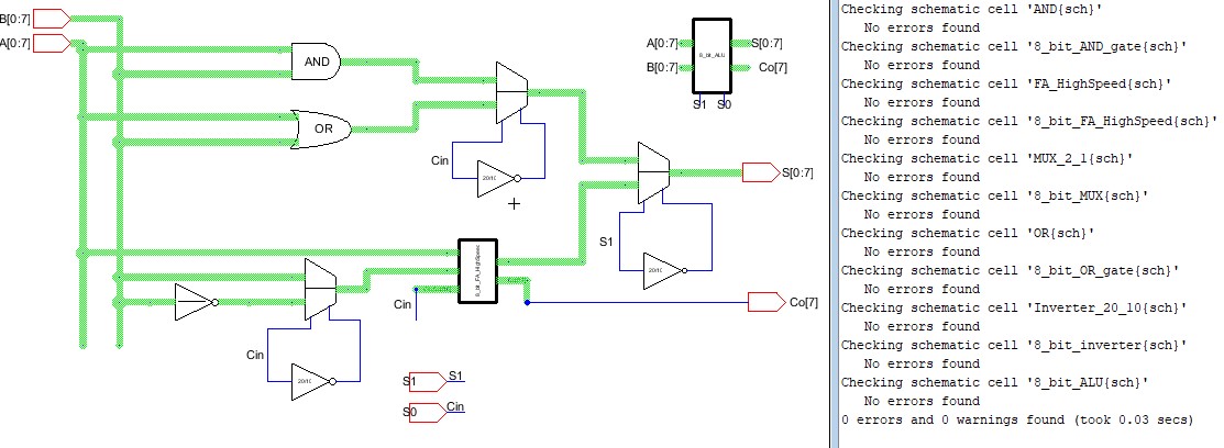
Figure 6. Schematic of 8-bit ALU and clean DRC.
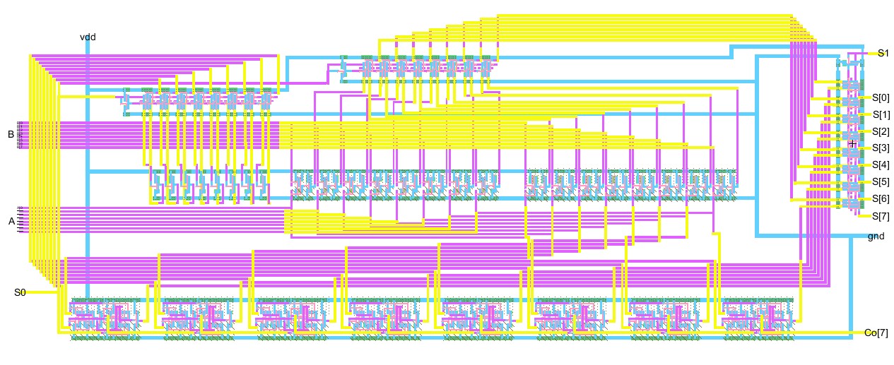
Figure 7. Layout of 8-bit ALU.
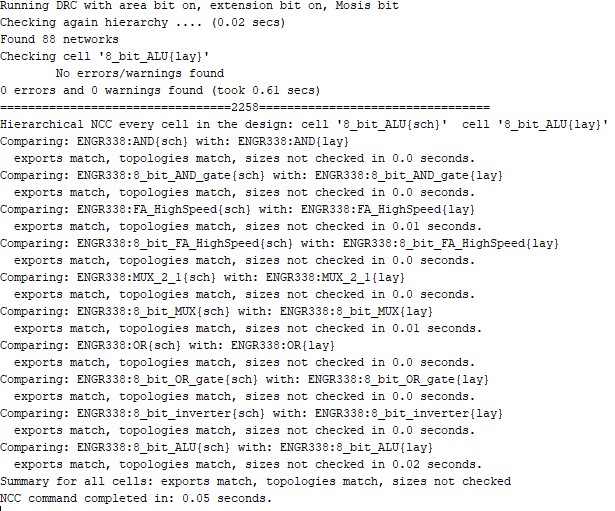
Figure 8. DRC and NCC of the 8-bit ALU.
Discussion:
By
completing this lab, we were able to gain more experience with
ElectriVLSI and create the schematic and layout of an 8-bit ALU. As
this is the final lab, I feel confident in my skills to use ElectriVLSI
to create schematics, icons, and layouts for any component. It is very
useful to be able to test the componets using LTSpice. I was
successfully able to complete all the tasks required using ElectriVLSI
and LTSpice. I think this lab took me the longest as it was very
tedious to wire up all the components and ensure that they follow the
standards within ElectriVLSI.