ENGR 338 2021 Spring
Lab 7: Using Buses in ElectriVLSI
Taylor Nakai
tsnakai@fortlewis.edu
Introduction:
In
this lab, we used ElectriVLSI to build a ring oscillator using buses
and to build multi-bit gates. We used LTSpice to create simulations for
the ring oscillator and muli-bit gates. The lab tasks required us to
build and simulate a ring oscillator, design and simulate an 8-bit AND gate, design and simulate an 8-bit OR gate, design and simulate an 8-bit NAND gate, and design and simulate an 8-bit NOR gate.
Task 1:
In
task 1, we were given the task to build and simulate a ring oscillator.
We used the inverter that we had previously created in Lab 4 and
connected 11 inverters in a row to form the ring. Once connected we
were able to run a simulation using LTSpice as shown in Figure 1. From
there we wanted to build it differently using data buses to create 11
inverters virtually and simulate it to see if it produces the same
results, which is shown in Figure 2. After we had finished the
schematic it was time to create the layout, and connect them in a ring
using Metal 1, Metal 2, and exporting the necessary ports as shown in
Figure 3. Using buses in the layout is not an option since at the
schematic level we are allowed to simplify and make the component more
concise, but at the layout level we have to specify every connection,
which won't allow us to use buses.
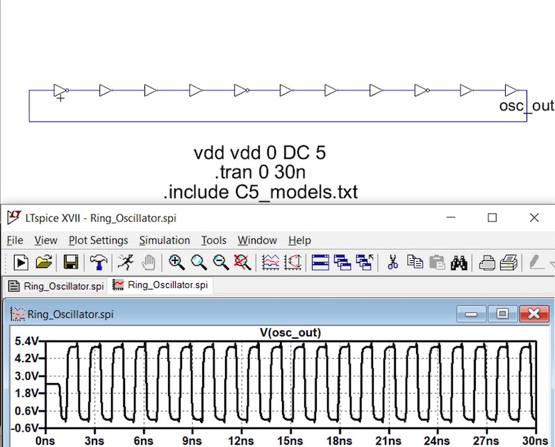
Figure 1. Ring oscillator and simulation using LTSpice.
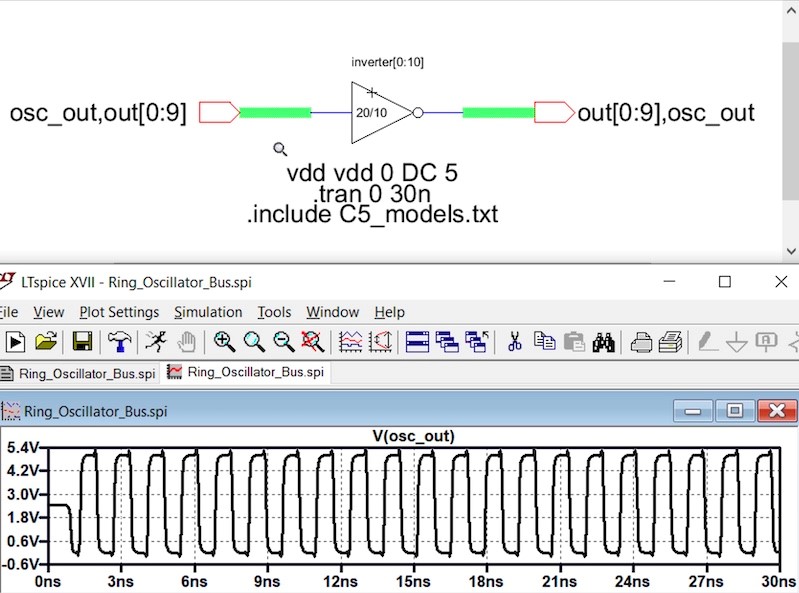
Figure 2. Ring oscillator using buses and simulation using LTSpice.
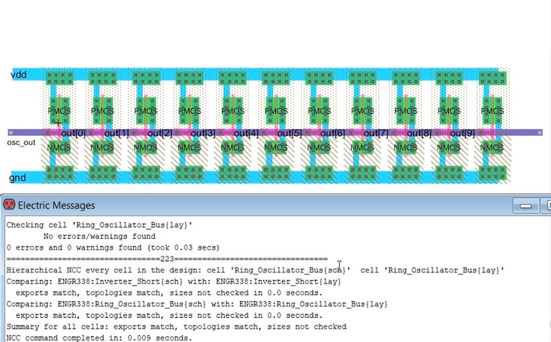
Figure 3. Layout of ring oscillator with clean DRC and NCC.
Task 2:
In
task 2, we were given the task of creating a 8-bit AND gate. Using the
NAND gate that we had previously created we were able to design the
schematic of the AND gate as shown in Figure 4. Once done with the
schematic we needed to create the layout, which is shown in Figure 5.
With the AND gate built we were able to use buses to create the 8-bit
AND gate, so we used the icon from the AND gate to build the schematic
of the 8-bit AND gate shown in Figure 6. To ensure that the 8-bit AND
gate was implemented correctly two simulations were ran using LTSpice
shown in Figure 7 and Figure 8. Once the logic was confirmed, the
layout of the 8-bit AND gate was created using the layout of the AND
gate as shown in Figure 9.
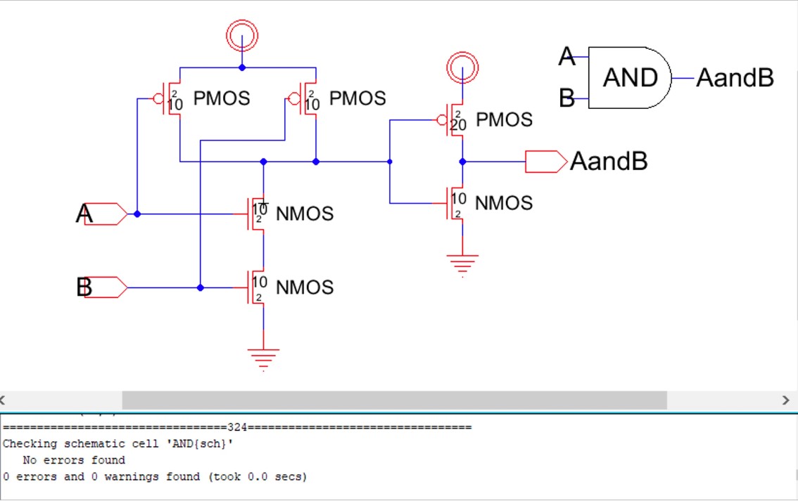
Figure 4. Schematic of AND gate with clean DRC.
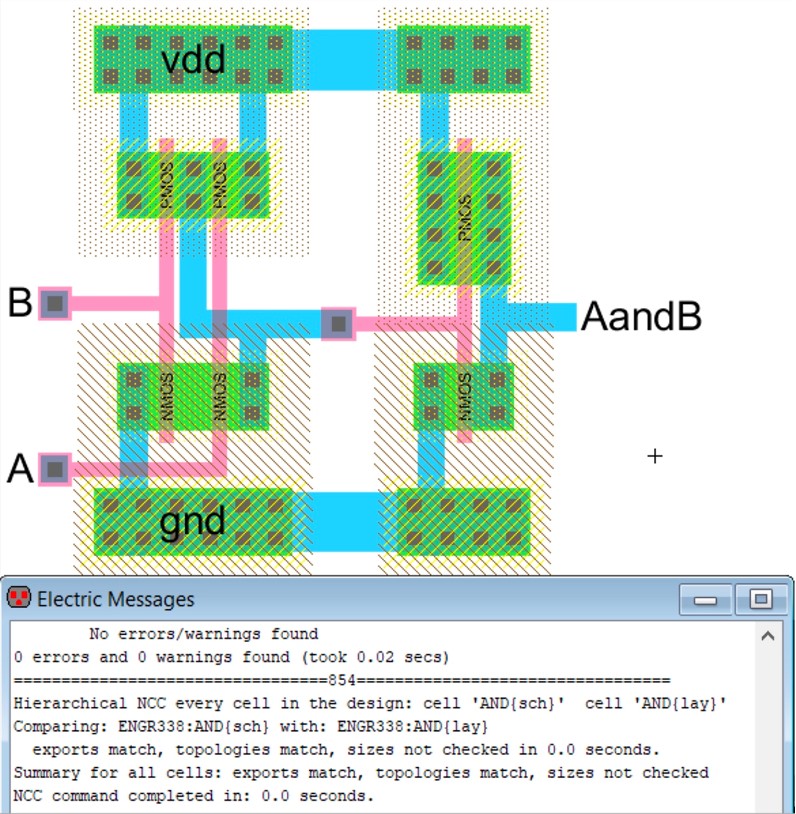
Figure 5. Layout of AND gate with clean DRC and NCC.
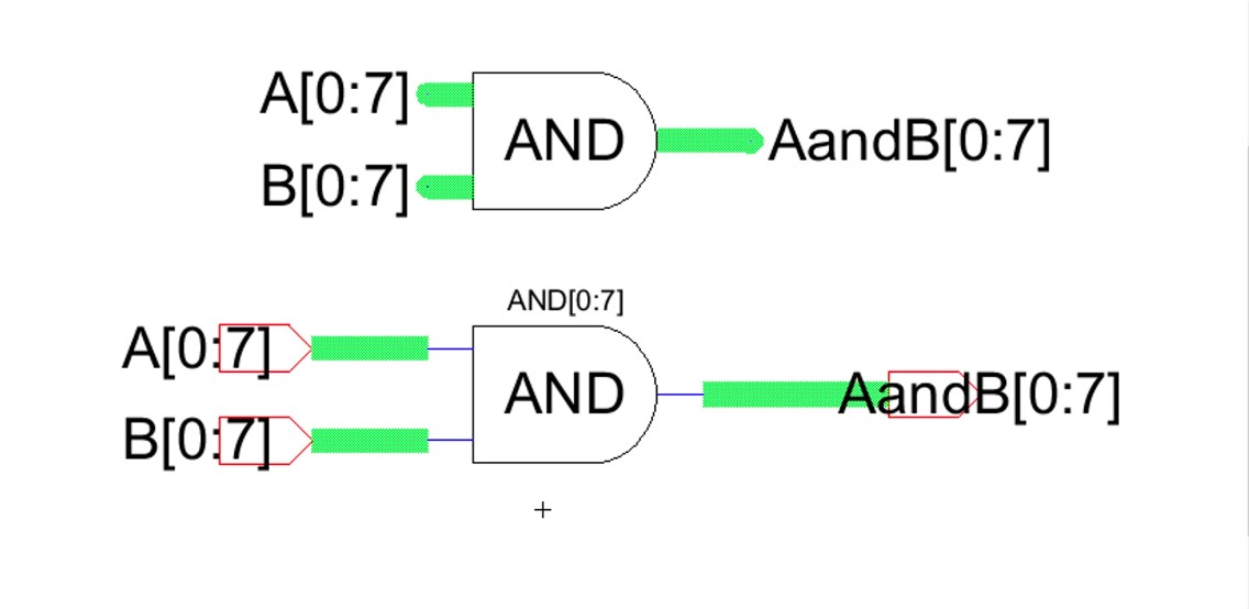
Figure 6. Schematic of 8-bit AND gate with icon.
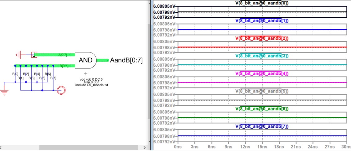
Figure 7. Simulation of 8-bit AND gate using LTSpice.
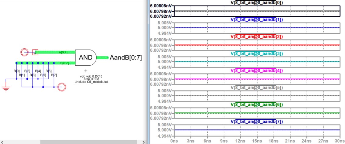
Figure 8. Simulation of 8-bit AND gate using LTSpice.
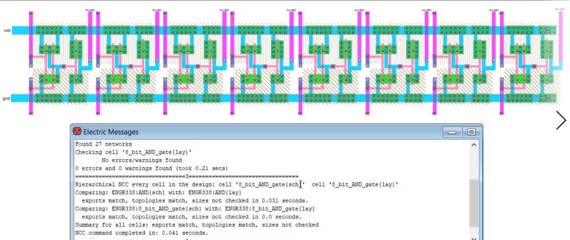
Figure 9. Layout of 8-bit AND gate with clean DRC and NCC.
Task 3:
In
task 3, we were given the task of creating a 8-bit OR gate. Using the
NOR gate that we had previously created we were able to design the
schematic of the OR gate as shown in Figure 10. Once done with the
schematic we needed to create the layout, which is shown in Figure 11.
With the OR gate built we were able to use buses to create the 8-bit OR
gate, so we used the icon from the OR gate to build the schematic
of the 8-bit OR gate shown in Figure 12. To ensure that the 8-bit OR
gate was implemented correctly two simulations were ran using LTSpice
shown in Figure 13 and Figure 14. Once the logic was confirmed, the
layout of the 8-bit OR gate was created using the layout of the OR
gate as shown in Figure 15.
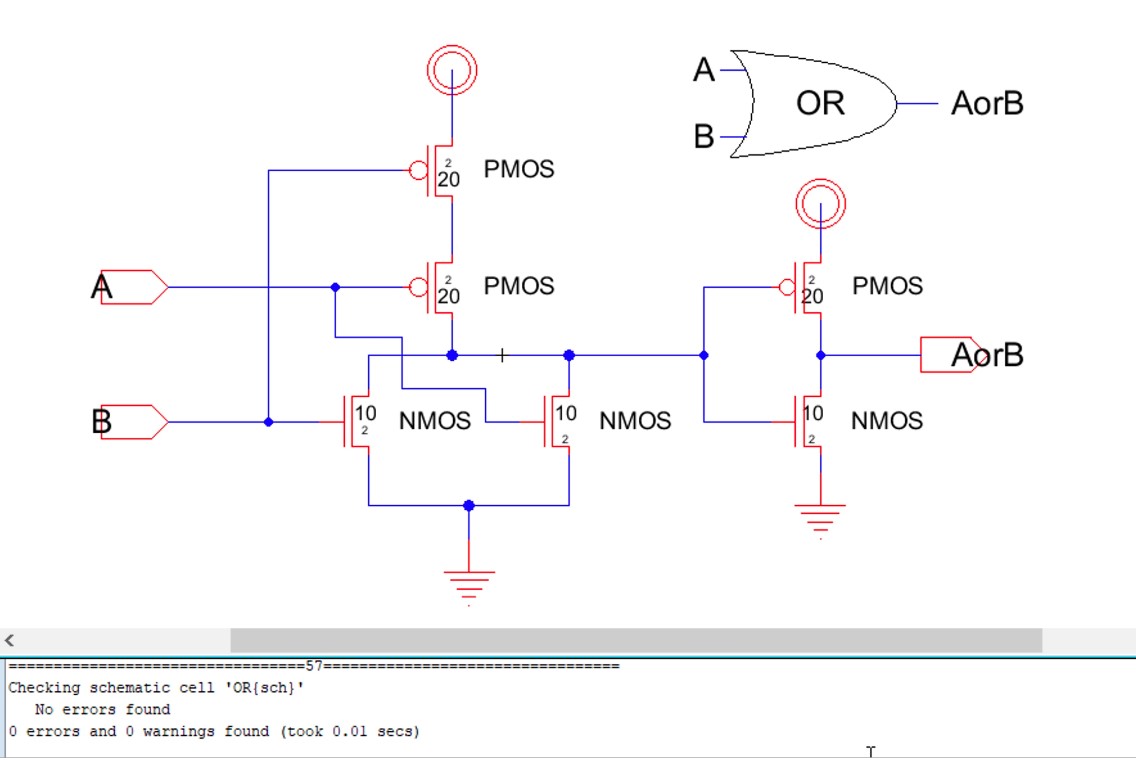
Figure 10. Schematic of OR gate with clean DRC.
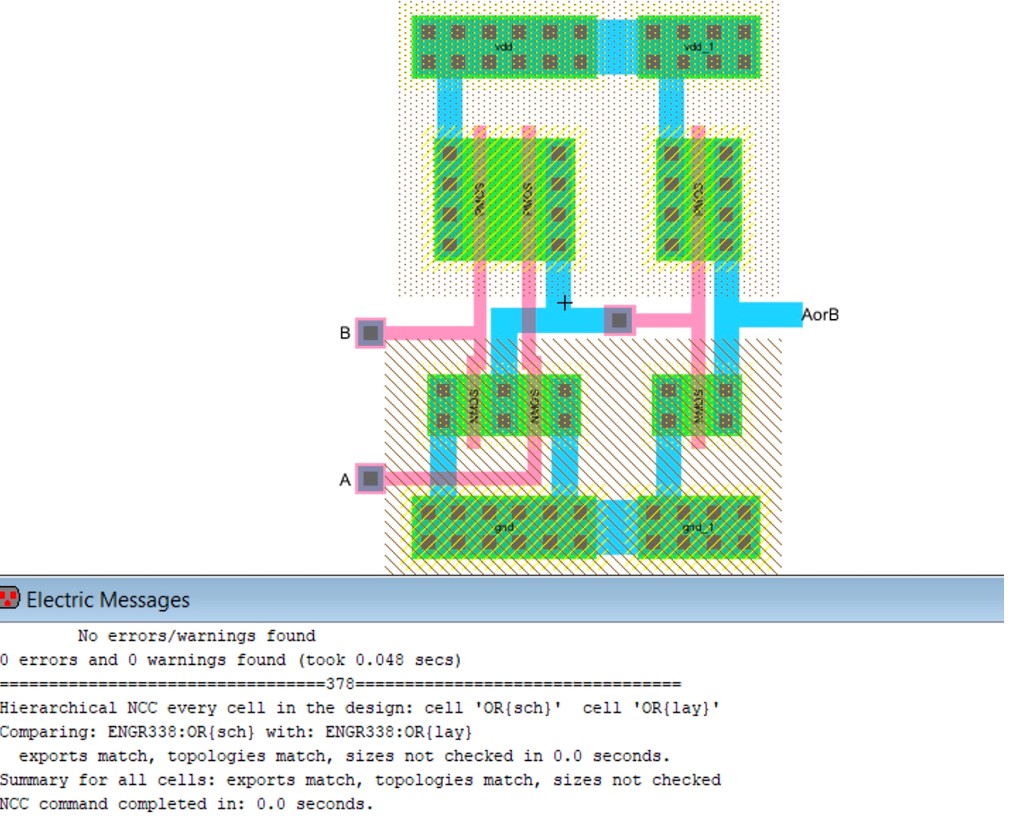
Figure 11. Layout of OR gate with clean DRC and NCC.
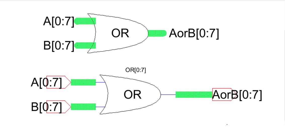
Figure 12. Schematic of 8-bit OR gate.
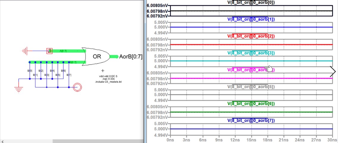
Figure 13. Simulation of 8-bit OR gate.
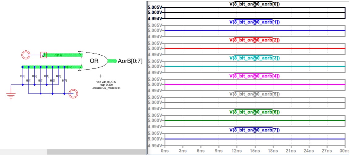
Figure 14. Simulation of 8-bit OR gate.
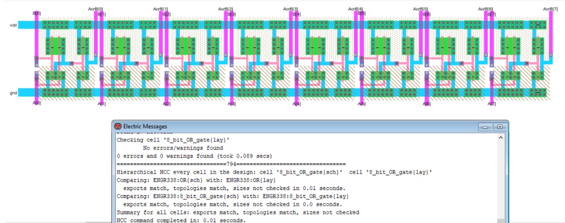
Figure 15. Layout of 8-bit OR gate with DRC and NCC.
Task 4:
In task 4, we were given the task of designing an 8-bit NAND gate. Using
the NAND gate that we had previously created we were able to design the
schematic of the 8-bit NAND gate shown in Figure 16. To ensure that the 8-bit NAND
gate was implemented correctly two simulations were ran using LTSpice
shown in Figure 17 and Figure 18. Once the logic was confirmed, the
layout of the 8-bit NAND gate was created as shown in Figure 19.
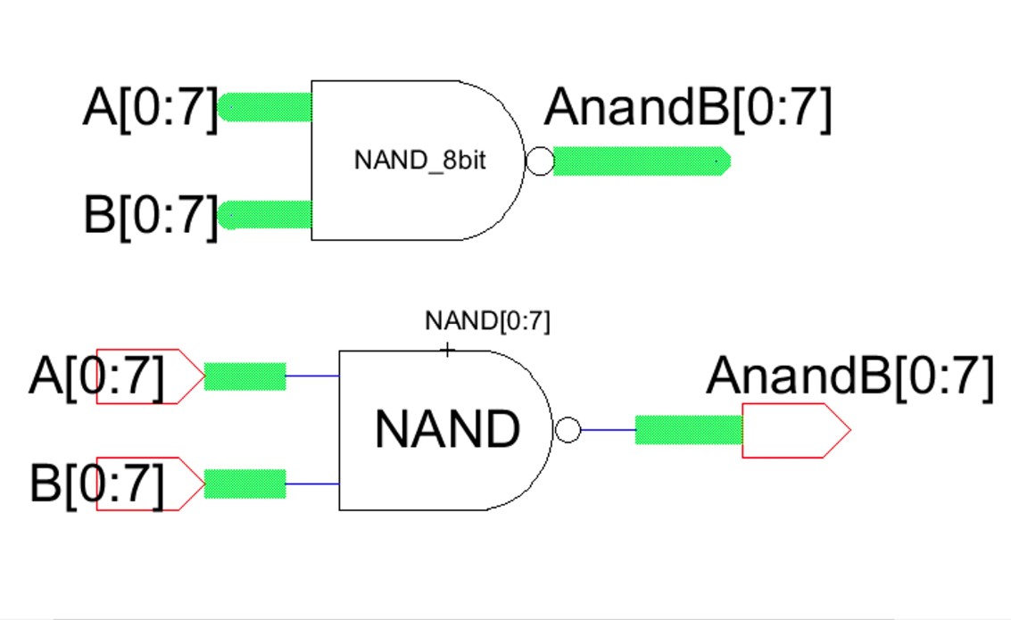
Figure 16. Schematic of 8-bit NAND gate.
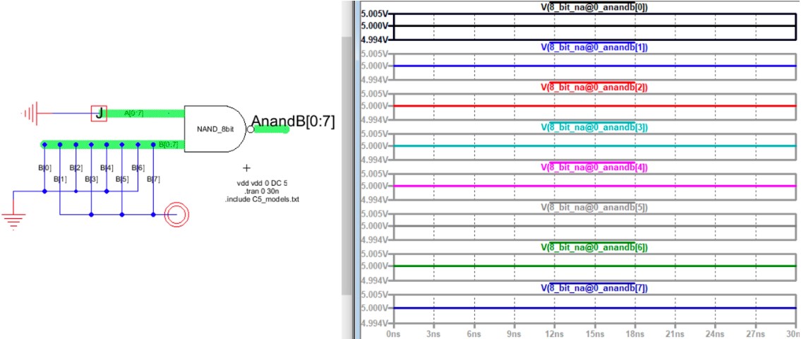
Figure 17. Simulation of 8-bit NAND gate using LTSpice.
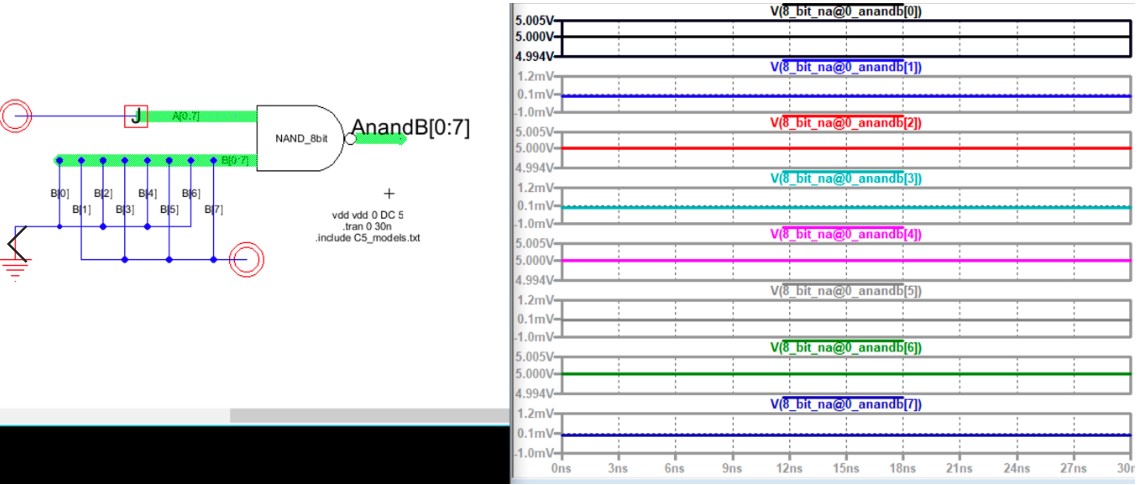
Figure 18. Simulation of 8-bit NAND gate using LTSpice.
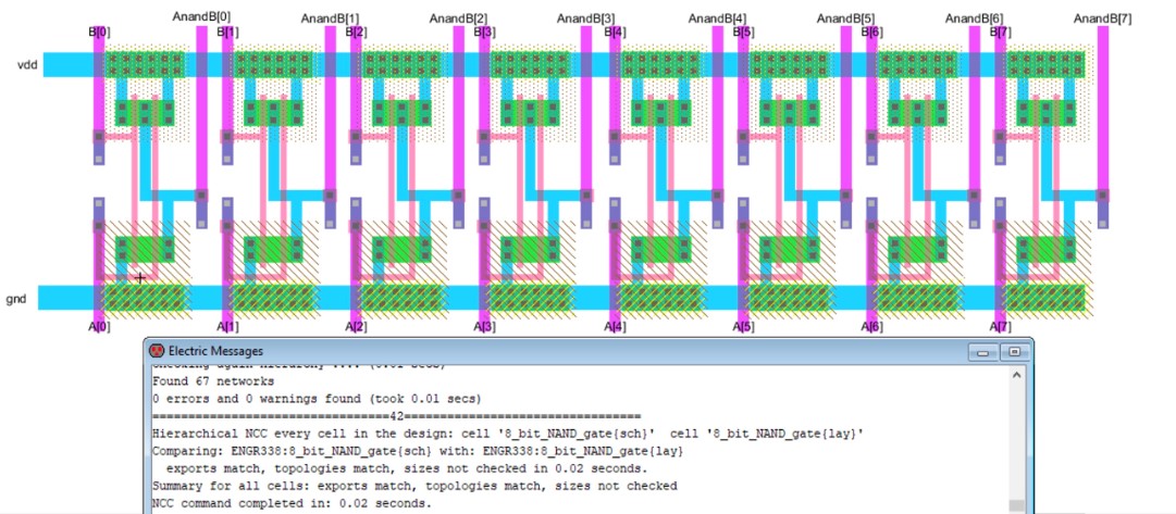
Figure 19. Layout of 8-bit NAND gate with DRC and NCC.
Task 5:
In task 5, we were given the task of designing an 8-bit NOR gate. Using
the NOR gate that we had previously created we were able to design the
schematic of the 8-bit NOR gate shown in Figure 20. To ensure that the 8-bit NOR
gate was implemented correctly two simulations were ran using LTSpice
shown in Figure 21 and Figure 22. Once the logic was confirmed, the
layout of the 8-bit NOR gate was created as shown in Figure 23.
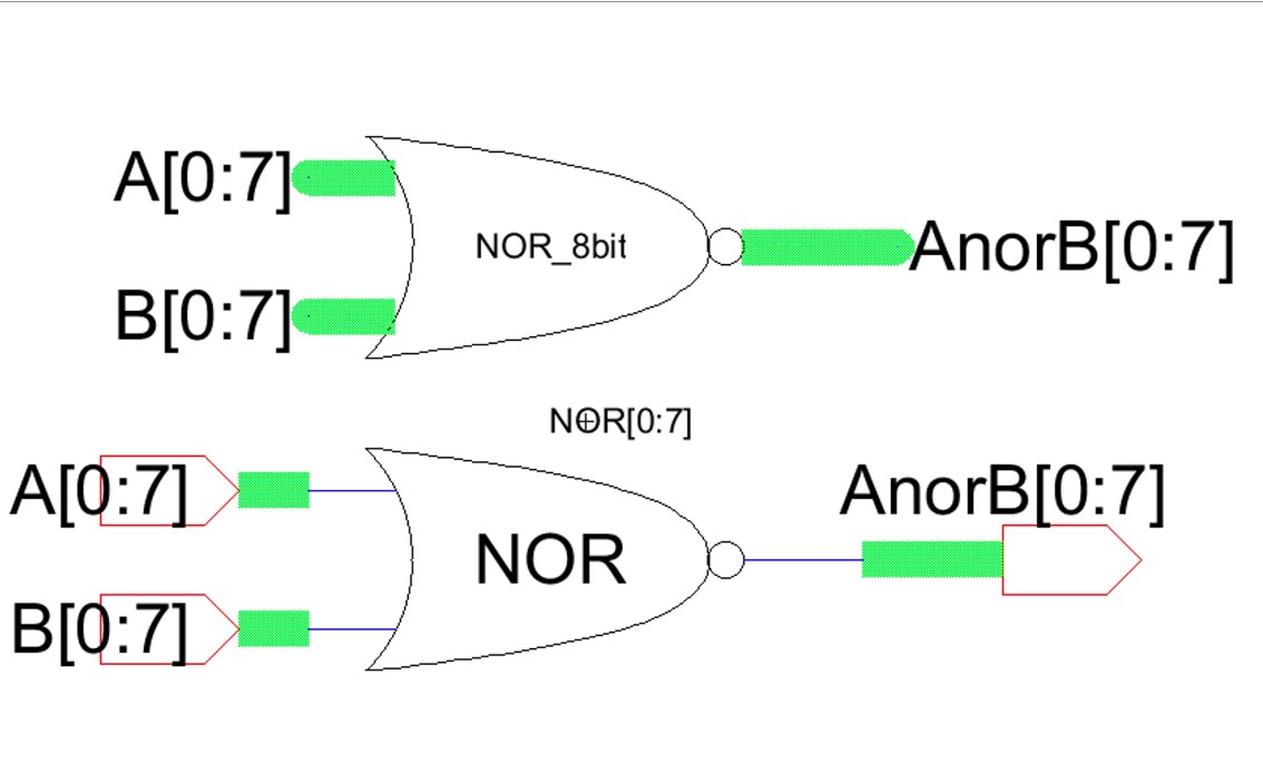
Figure 20. Schematic of 8-bit NOR gate.
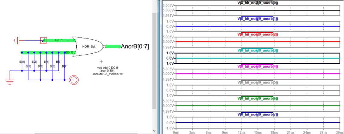
Figure 21. Simulation of 8-bit NOR gate using LTSpice.
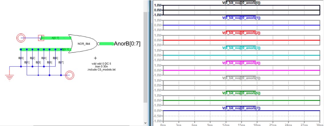
Figure 22. Simulation of 8-bit NOR gate using LTSpice.
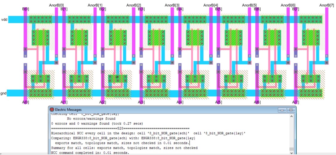
Figure 23. Layout of 8-bit NOR gate with DRC and NCC.
Discussion:
By
completing this lab, we were able to gain more experience using
ElectriVLSI, design a ring oscillator, and using buses to create
multi-bit gates. I was successfully able to complete all the tasks
required using ElectiVLSI and LTSpice. This lab was interesting as it
allowed us to use the single gates that we created to build multi-bit
gates using buses. Unfortunately, buses can only be used at the
schematic level of the design and not at the layout level where we
still have to specify every connection. Since it is not possible to use
buses at the layout level it took more time to create the layouts than
it did to create the schematic. I feel that what I have learned in this
lab will come in handy in the future.