ENGR 338 2021 Spring
Lab 6: Build a NAND, NOR, XOR, and Full Adder
Taylor Nakai
tsnakai@fortlewis.edu
Introduction:
In
this lab, we used ElectriVLSI to create to build a NAND, NOR, XOR, and
Full Adder. For the NAND, NOR, and XOR gates we had to build the
schematic using NMOS and PMOS transitors, created the icon for the
gate, and use nAct, pAct, pWell, nWell, pMos, and nMos to create the
layout. We also used LTSpice to test the schematics with using
simulations to ensure that they were properly implemented. Using the
NAND, NOR, XOR, and Inverter from previous lab, we were able to build
the schematic and layout of the Full Adder.
Task 1:
In
task 1, we were given the task of creating the schematic, icon, and
layout of the NAND gate. We had to first create the schematic using a
combination of NMOS and PMOS transistors, as seen in Figure 1. After we
had the schematic completed we needed to design the icon for the NAND
gate. Once the schematic and icon were completed we had to test it
before creating the layout, so we used LTSpice to run a simulation to
test the logic, as seen in Figure 2. Finally we were able to design the
layout of the NAND gate and ran both a DRC and NCC check to make sure
everything had been connected and the schematic and layout matched each
other, as shown in Figure 3.
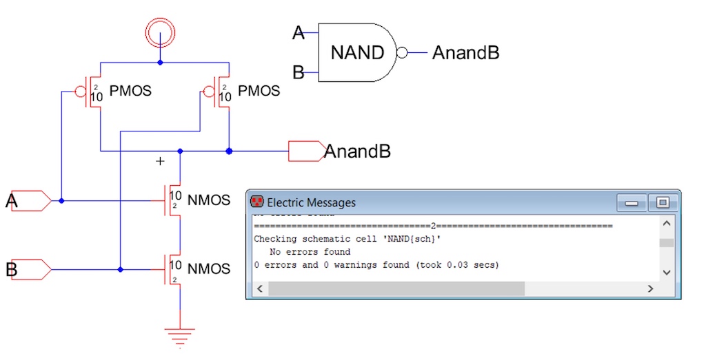
Figure 1. Schematic of NAND gate using PMOS and NMOS transistors with DRC check.
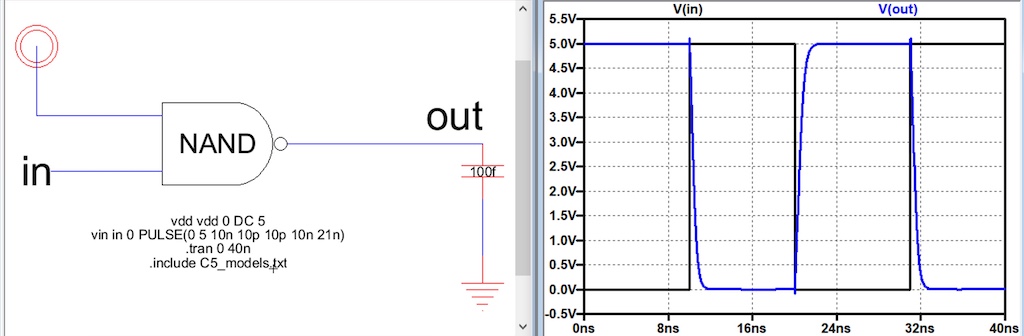
Figure 2. Simulation of NAND gate using LTSpice to test the logic.
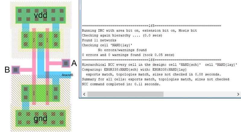
Figure 3. Layout of NAND gate and showing the results of the DRC and NCC checks.
Task 2:
In
task 2, we were given the task of creating the schematic, icon, and
layout of the NOR gate. We had to first create the schematic using a
combination of NMOS and PMOS transistors, as seen in Figure 4. Next
after the schematic was completed we needed to design the icon for the
NOR
gate. Once the schematic and icon were completed we had to test it
before creating the layout, so we used LTSpice to run a simulation to
test the logic, as seen in Figure 5. This allow us to design the
layout of the NOR gate and ran both a DRC and NCC check to make sure
everything had been connected and the schematic and layout matched each
other, as shown in Figure 6.
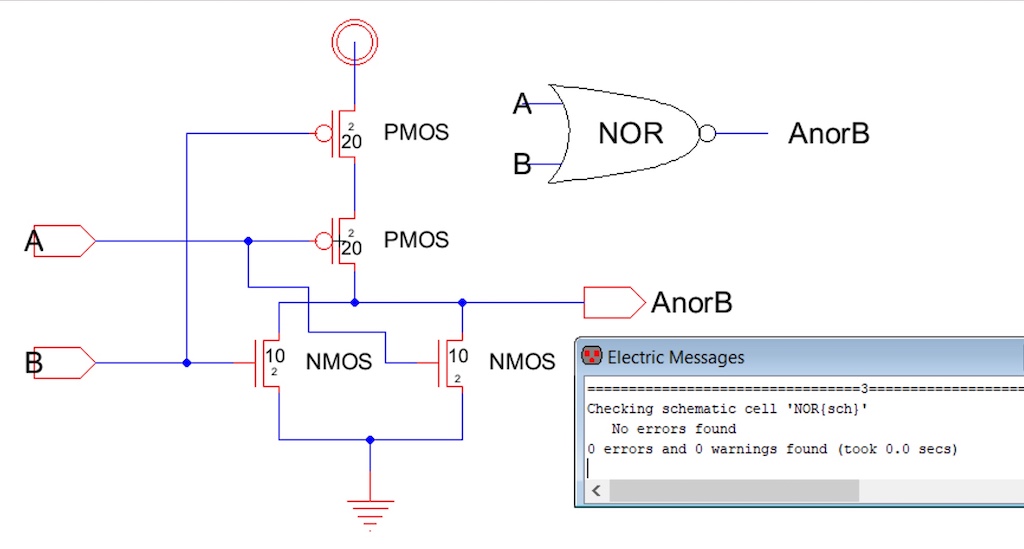
Figure 4. Schematic of NOR gate using PMOS and NMOS transistors with DRC check.
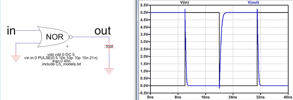
Figure 5. Simulation of NOR gate using LTSpice to test the logic.
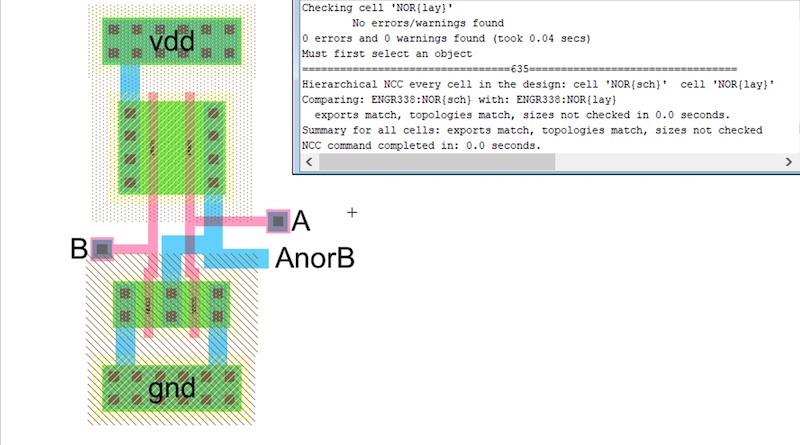
Figure 6. Layout of NOR gate and showing the results of the DRC and NCC checks.
Task 3:
In
task 3, we were given the task of creating the schematic, icon, and
layout of the XOR gate. First, we created the schematic using a
combination of NMOS and PMOS transistors, as seen in Figure 7. With the
schematic being completed we needed to design the icon for the XOR
gate. In order to verify that the schematic was created successfully,
we used LTSpice to test the logic of the XOR gate, as shown in Figure 8
and 9. Once the schematic was verified, we were able to design the
layout of the XOR gate. To check the implementation of the XOR gate we
checked it against the stick diagram shown in Figure 10 and ran both a
DRC and NCC check to make sure
everything had been connected and the schematic and layout matched each
other, as shown in Figure 11.
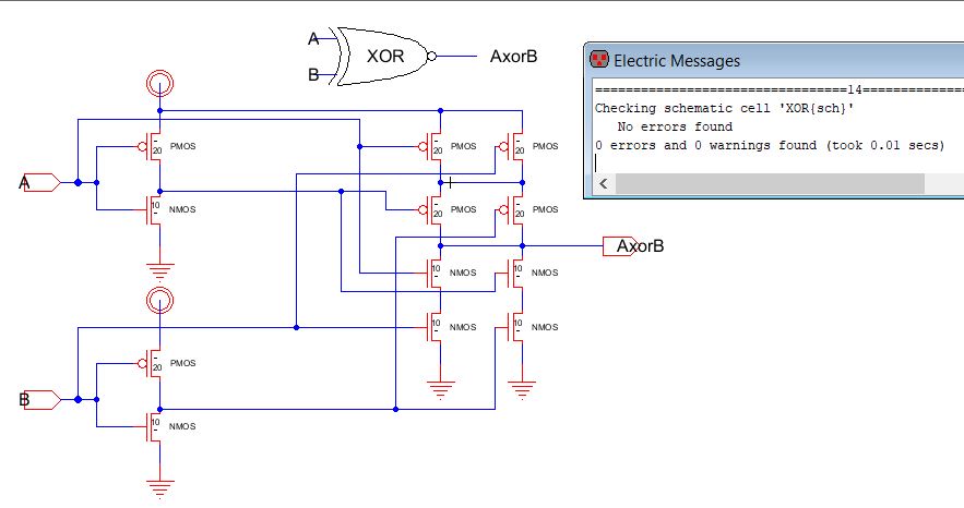
Figure 7. Schematic of XOR gate using PMOS and NMOS transistors with DRC check.
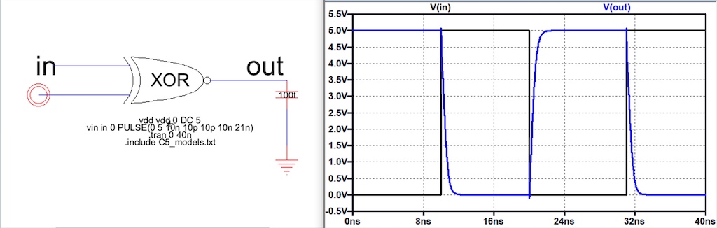
Figure 8. First simulation using VDD as one input of XOR gate using LTSpice to test the logic.
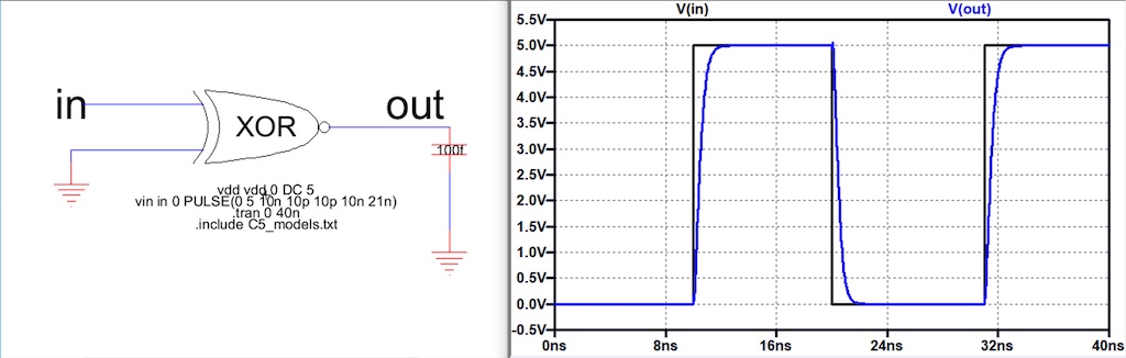
Figure 9. First simulation using GND as one input of XOR gate using LTSpice to test the logic.
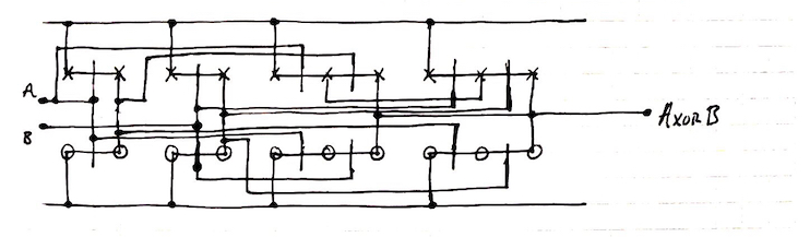
Figure 10. Stick diagram of XOR gate to help and check implementation of layout.
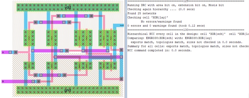
Figure 11. Layout of XOR gate and showing the results of the DRC and NCC checks.
Task 4:
In
task 4, we needed to design, simulate, and create the schematic and
layout of a full adder. The full adder's schematic was given to use as
it was derived in a previous class. Following the schematic we used the
NAND, NOR, XOR, and inverter that we had previously created to bulid
the full adder's schematic and ran a DRC to check for errors as seen in
Figure 12. After the schematic was built we created the symbol so we
could used it to test the logic as shown in Figure 13 and 14. Once that
was completed, we used all the gates and inverters that we had created
previously to create the layout of the full adder, which can be seen in
Figure 15.
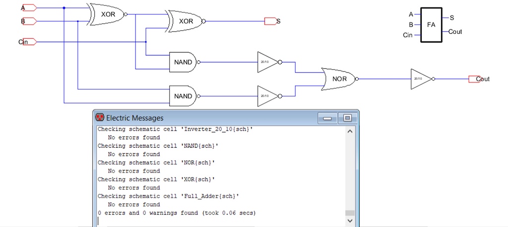 Figure 12. Schematic of full using previous gates and inverter with DRC check.
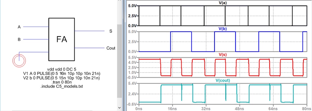
Figure 13. First simulation of full adder using VDD as Cin using LTSpice to test the logic.
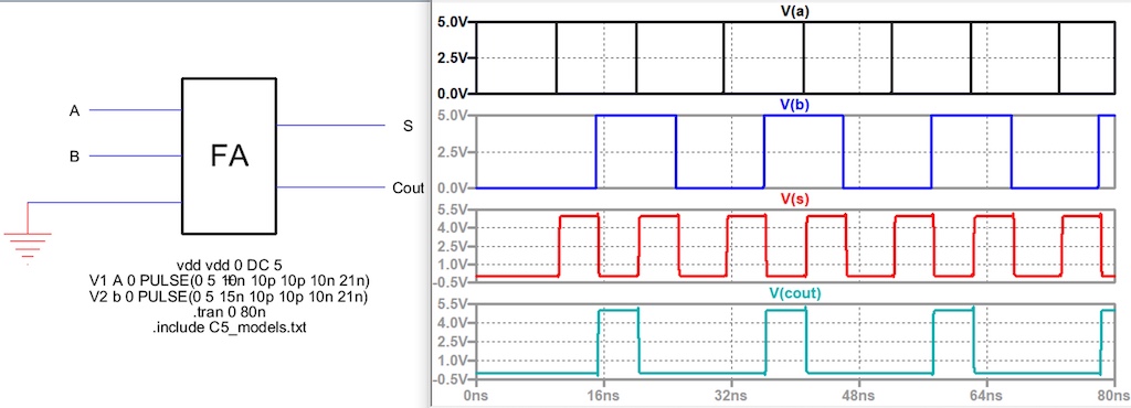
Figure 14. First simulation of full adder using GND as Cin using LTSpice to test the logic.
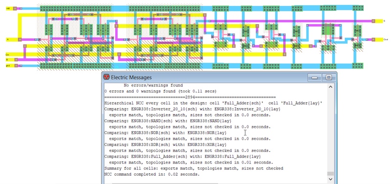
Figure 15. Layout of full adder and showing the results of the DRC and NCC checks.
Discussion:
By
completing this lab, we were able to gain more experience with
ElectriVLSI, create the layout and schematics of NAND gate, NOR gate,
XOR gate, and full adder, and use LTSpice to perform simulations. I was
successfully able to complete all the tasks required using ElectriVLSI
and LTSPICE. This was a lab that took A LOT of patience and was a good
learning experience as it required you to understand what was going on.
It feels like I am becoming more and more comfortable with ElectriVLSI
and LTSpice after every lab.