ENGR 338 2021 Spring
Lab 5: The Inverter
Taylor Nakai
tsnakai@fortlewis.edu
Introduction:
In
this lab, we used ElectriVLSI to create the schematic and layout of an
20/10 and 100/50 inverter. With the inverters we were able to perform
simulations using LTSpice, ALS, and IRSIM. The lab tasks required us to
create a schematic of the inverter, create a layout of the inverter,
use the multiplier function to build a larger inverter, run simulations
to verify the capabilities of the two inverters created, and use ALS
and IRSIM to perform simulations.
Task 1:
In
task 1, we were given the task to create a schematic of the 20/10
inverter. To begin we needed to use vdd symbol, gnd symbol, ports, a
PMOS transistor, and a NMOS transistor to be able to create the
schematic shown in Figure 1. To check if the implementation of the
inverter was done correctly a simulation was conducted to determine if
the input is inverted, as shown in Figure 2. After the inverter was
checked, we wrote the spice for a transient simulation using the
PULSE() input, which the code is shown in Figure 3 and the result is
shown in Figure 4.
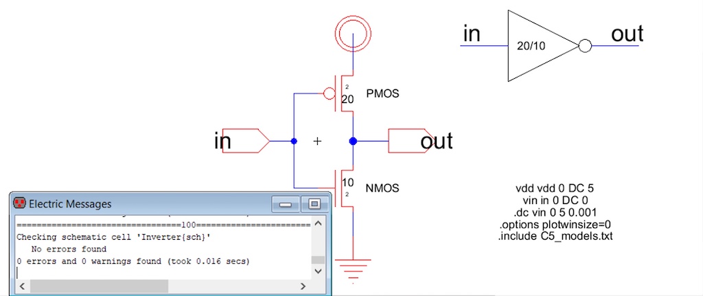
Figure 1. Schematic and Icon of 20/10 inverter with DRC check showing no errors.
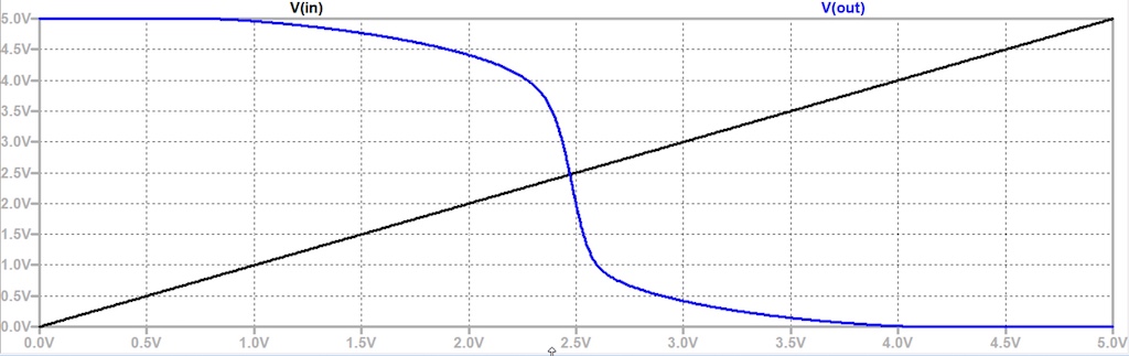
Figure 2. Simulation of 20/10 inverter showing that it inverts the input.
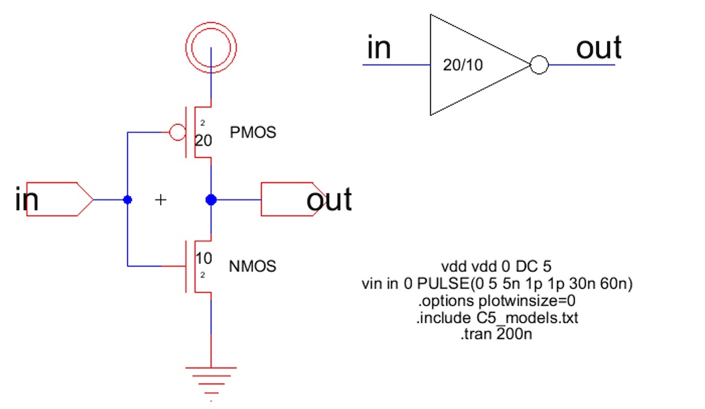
Figure 3. Schematic of 20/10 inverter showing the spice code for a PULSE() input.
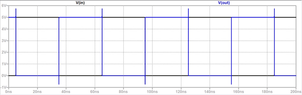 Figure 4. Simulation of 20/10 inverter with PULSE() input.
Task 2:
In
task 2, we were given the task of creating the layout of the inverter.
To create the layout of the inverter, we had to use a nWell, 2 pAct, a
pMos, 2 nAct, a nMos, and a pWell. After making all the correct
connections and exporting in, out, gnd, and vdd, we ran a DRC and NCC
check to ensure everthing was done correctly. The result of the layout
of the inverter is shown in Figure 5.
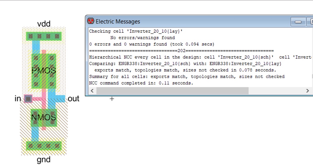
Figure 5. Layout of the 20/10 inverter with DRC and NCC checks to showing no errors.
Task 3:
In
task 3, we were given the task of using the multiplier function to
build a larger inverter (100/50). Using a duplicate of the 20/10
inverter built in task 1, we used the multiplier function to add 5
parallel PMOS and NMOS transistors, as shown in Figure 6. After the
schematic was completed for the 100/50 inverter, we needed to duplicate
and modify the layout created in task 2. We had to add 5 PMOS, 5 NMOS,
and modify the dimensions of the nWell and pWell of the layout, which
the result is shown in Figure 7. A DRC and NCC check was ran to ensure
that everything was done correctly, which can also be shown in Figure 7.
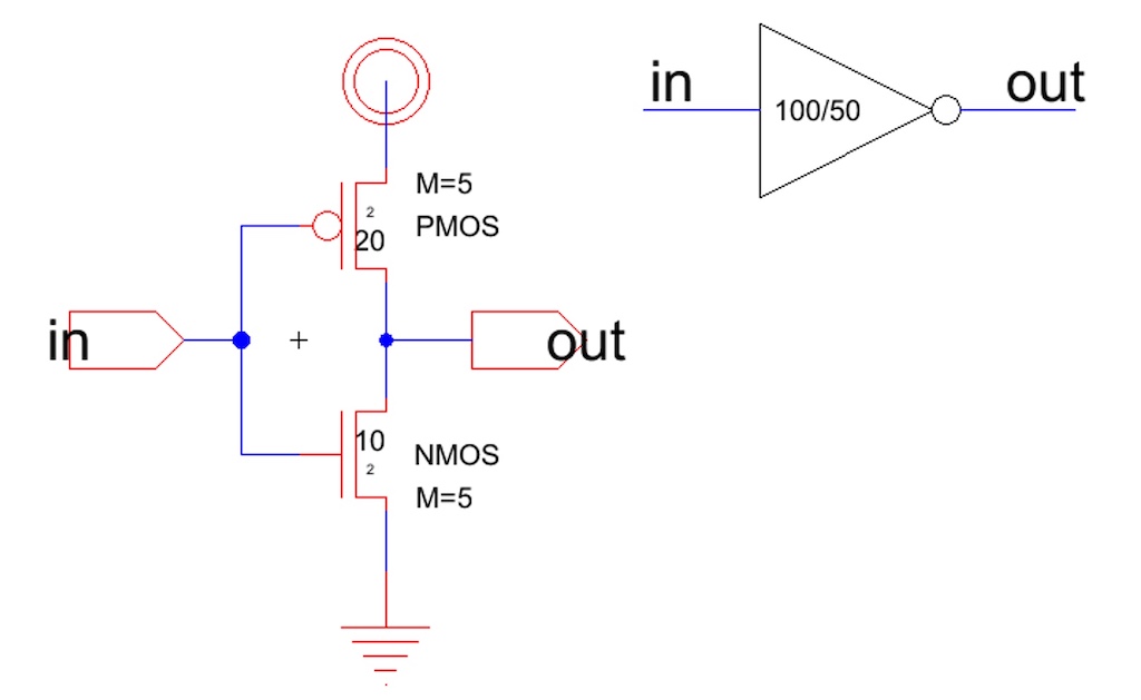
Figure 6. Schematic of 100/50 inverter using multiplier function.
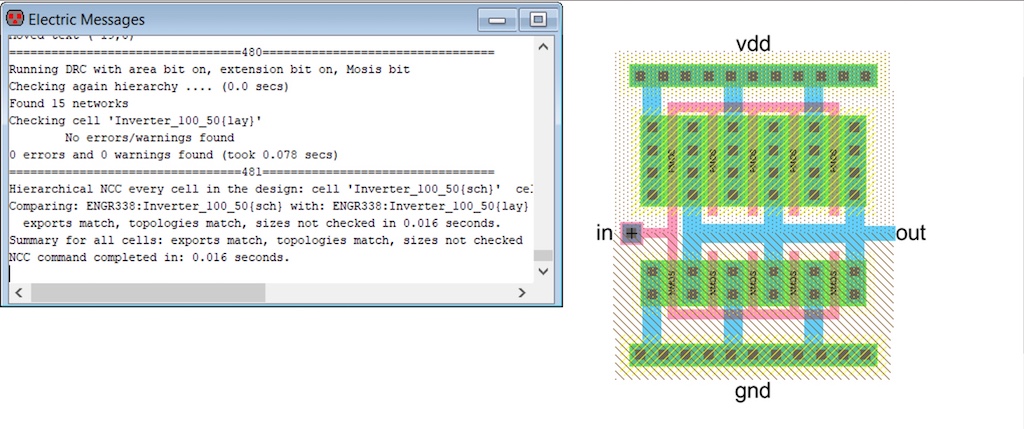
Figure 7. Layout of 100/50 inverter with DRC and NCC checks showing no erros.
Task 4:
In
task 4, we were given the task to verify the driving capabilites of the
20/10 and 100/50 inverters by running 3 different simulations to drive
a 100fF, 1pF, and 10pF capacitor. For the 3 simulations using the 20/10
inverter, the schematics were created then the simulation was completed
using LTSpice, the results of the 20/10 simulations can be seen in
Figures 8-10. For the 3 simulations using
the 100/50 inverter, the schematics were created then the simulation was
completed using LTSpice, the results of the 100/50 simulations can be
seen in Figures 11-13.
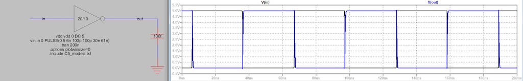
Figure 8. Schematic of 20/10 inverter using a capacitor (100f) as the load and simulation ran in LTSpice.
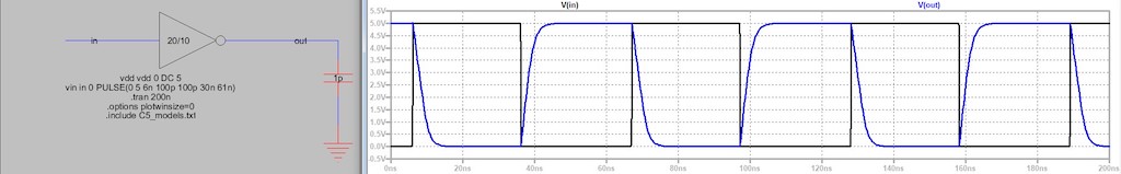
Figure 9. Schematic of 20/10 inverter using a capacitor (1p) as the load and simulation ran in LTSpice.
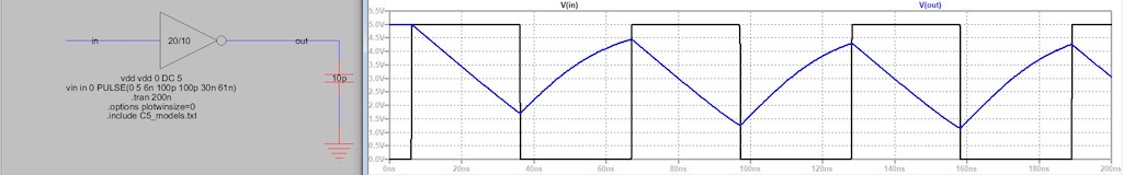
Figure 10. Schematic of 20/10 inverter using a capacitor (10p) as the load and simulation ran in LTSpice.
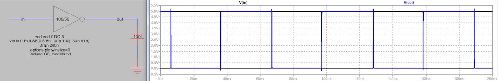
Figure 11. Schematic of 100/50 inverter using a capacitor (100f) as the load and simulation ran in LTSpice.
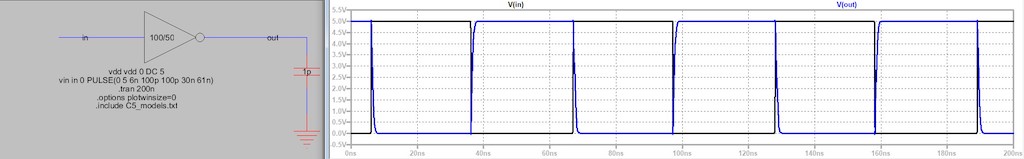
Figure 12. Schematic of 100/50 inverter using a capacitor (1p) as the load and simulation ran in LTSpice.
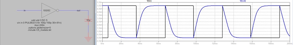
Figure 13. Schematic of 100/50 inverter using a capacitor (10p) as the load and simulation ran in LTSpice.
Task 5:
In
task 5, we were given the task of using different simulation tools like
ALS and IRSIM. To begin we needed a schematic to conduct the
simulations with so we build a schematic using both inverters as shown
in Figure 14. Using ALS, we ran a simulation and set the input signal
and got immediate results of the 2 out signals, as shown in Figure 15.
Using IRSIM, we ran a simular simulation to the ALS simulation but
noticed that in IRSIM there was a noticable delay, as shown in Figure
16.
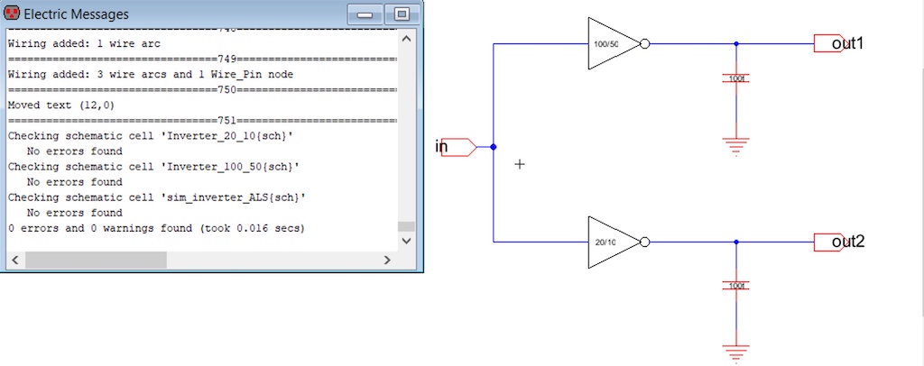
Figure 14. Schematic using a 100/50 inverter and 20/10 inverter with a clean DRC.
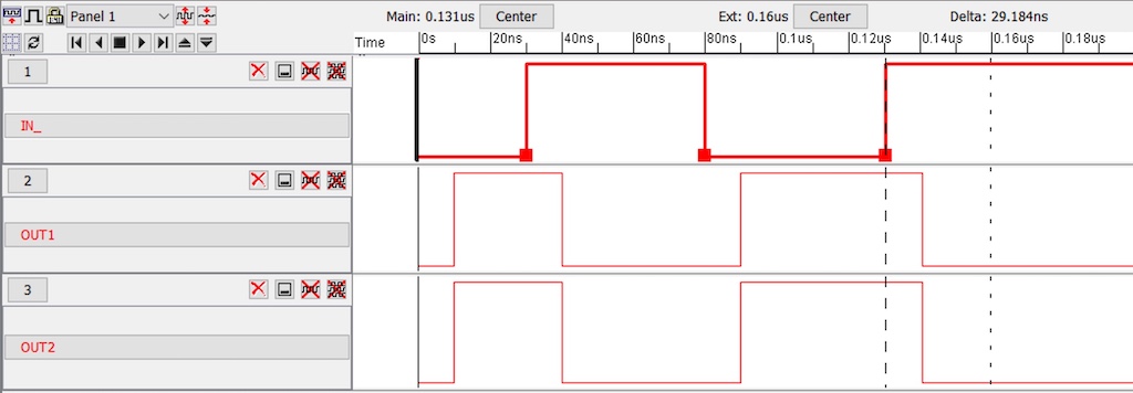
Figure 15. Results from ALS simulation using IN to toggle the signal.
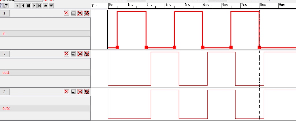
Figure 16. Results from IRSIM simulation showing the different delay times.
Discussion:
By
completing this lab, we were able to gain more experience with
ElectriVLSI, create a schematic and layout for an inverter, and perform
simulations using LTSpice, ALS, and IRSIM. I was successfully
able to complete all the task required using ElectriVLSI and LTSpice.
This was an interesting lab and I felt that this lab was useful with
learning how to create an inverter using the NMOS and PMOS transistors
that we have been working with in previous labs.