ENGR 338 2021 Spring
Lab 4: MOSFETs and IV Curves
Taylor Nakai
tsnakai@fortlewis.edu
Introduction:
In
this lab, we used ElectriVLSI to build MOSFETs and were able to run
simulations to analyse the IV curves of the MOSFETs created. The lab
tasks required us to create a NMOS and PMOS transistors using the C5
technology, creating both a schematic and layout view. Once the
transistors had been created we were able to simulate the IV curves in
LTSpice.
Task:
In
this task, we were given the task of creating the NMOS and PMOS
transistors in ElectriVLSI. To begin we needed to create the NMOS and
PMOS transistor schematics, as seen in Figure 1 and Figure 7. We also
needed to create the NMOS and PMOS transistor layouts, as seen in
Figure 3 and Figure 9. Once we had the schematic and layout for the
NMOS and PMOS, a NCC test was conducted to ensure that the schematic
matched the layout, as seen in Figure 2 and Figure 8. We also ran
an ERC and DRC check to make sure that our designs were implemented
correctly, as seen in Figure 4 and Figure 10. Finally we were able to
perform the simulations for the NMOS and PMOS transistors using LTSpice
and the results of the NMOS transistor is shown in Figure 5 and the
results of the PMOS transistor is shown in Figure 11. We also performed
simulations using the schematics as shown in Figure 6 and Figure 12.
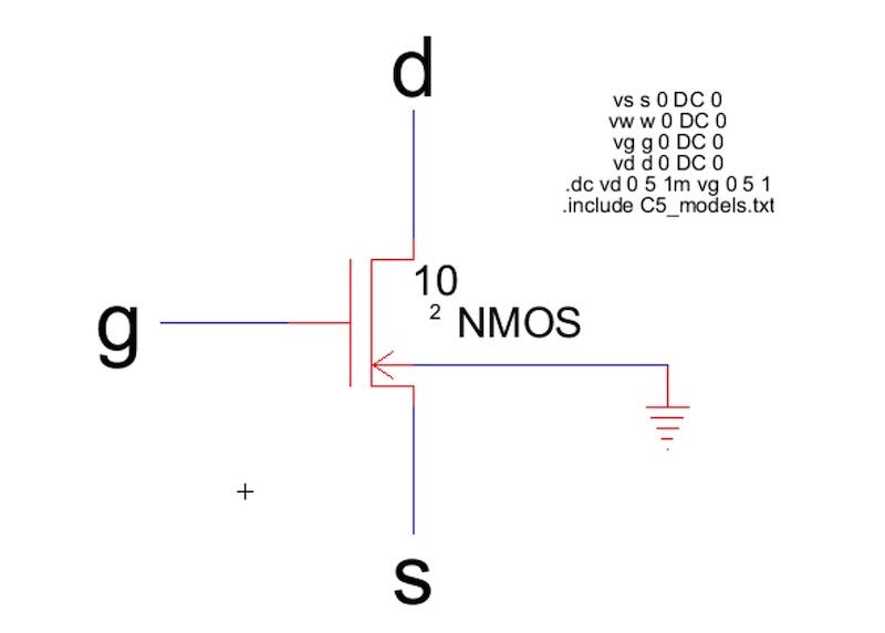
Figure 1. Schematic view of the NMOS transistor.
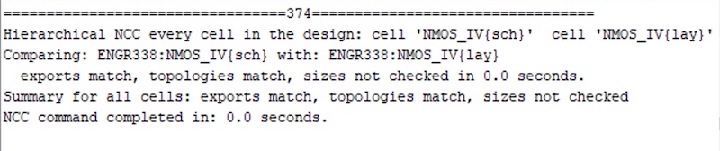
Figure 2. NCC to verify the NMOS schematic matches the layout.
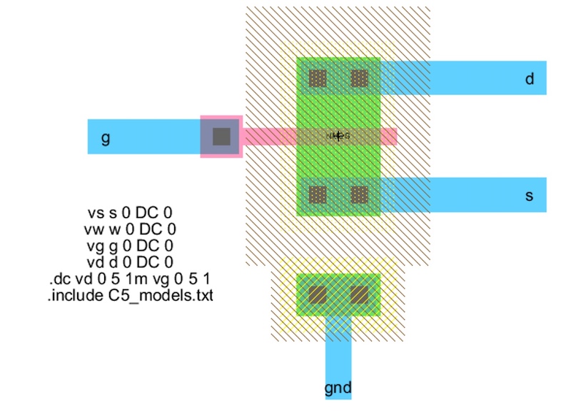
Figure 3. Layout view of the NMOS transistor.
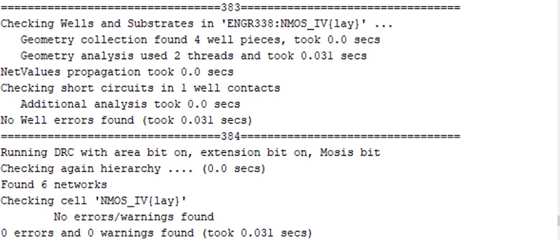
Figure 4. ERC and DRC of NMOS design.
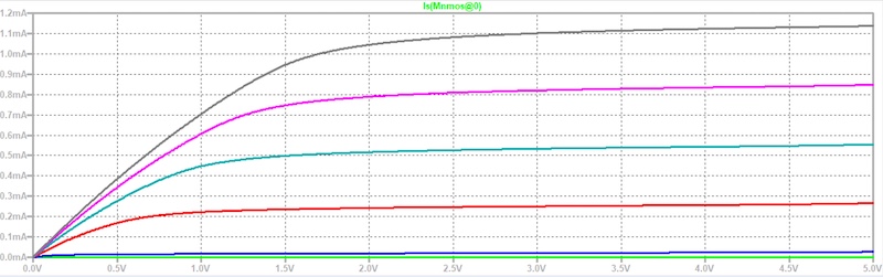
Figure 5. Simulation results from the NMOS transistor in LTSpice using the NMOS layout.
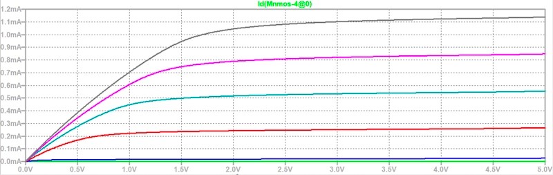
Figure 6. Simulation results from the NMOS transistor in LTSpice using the NMOS schematic.

Figure 7. Schematic view of the PMOS transistor.
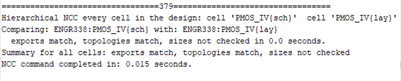
Figure 8. NCC to verify the PMOS schematic matches the layout.
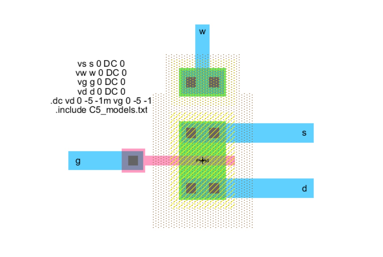
Figure 9. Layout view of the PMOS transistor.
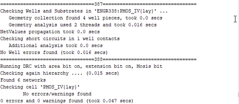
Figure 10. ERC and DRC of PMOS design.
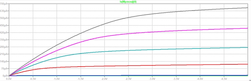
Figure 11. Simulation results from the PMOS transistor in LTSpice using the PMOS layout.
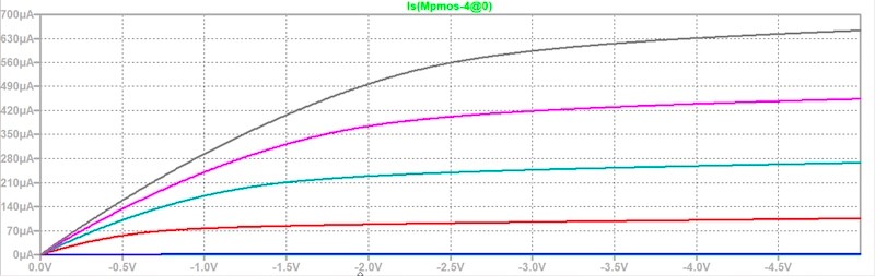
Figure 12. Simulation results from the PMOS transistor in LTSpice using the PMOS schematic.
Discussion:
By completing this lab, we
were able to gain more experience with ElectriVLSI, build schematics
and layouts, build MOSFETs, and were able to run simulations using
LTSpice. We were successfully able to use ElectriVLSI to build MOSFETs
and were able to run simulations to analyse the IV curves of the
MOSFETs created. I felt that this lab was helpful with learning more
about the NMOS and PMOS transistors.