ENGR 338 2021 Spring
Lab 3: Layout the R-2R DAC
Taylor Nakai
tsnakai@fortlewis.edu
Introduction:
In
this lab, we used ElectriVLSI to create the layout for the R-2R DAC
using N-Well resistors and became more familiar with ElectriVLSI and
LTSpice for integrated circuit (IC) design. The two tasks that we had
to complete were to create a schematic of the subcells for the R-2R
ladder and create the layout of the subcells for the R-2R ladder.
Task 1:
In task 1, we
had to complete were to create a schematic of the subcells for the R-2R
ladder. To begin we had to create a subcell for the repeating structure
and create a icon, as shown in Figure 1, so that when the layout is
created you can can use the subcell for convenience. Once the subcell
schematic had been created we created a new schematic' R_2R_Ladder_v2' and used the icon to create the R-2R Ladder, as shown in Figure 2.
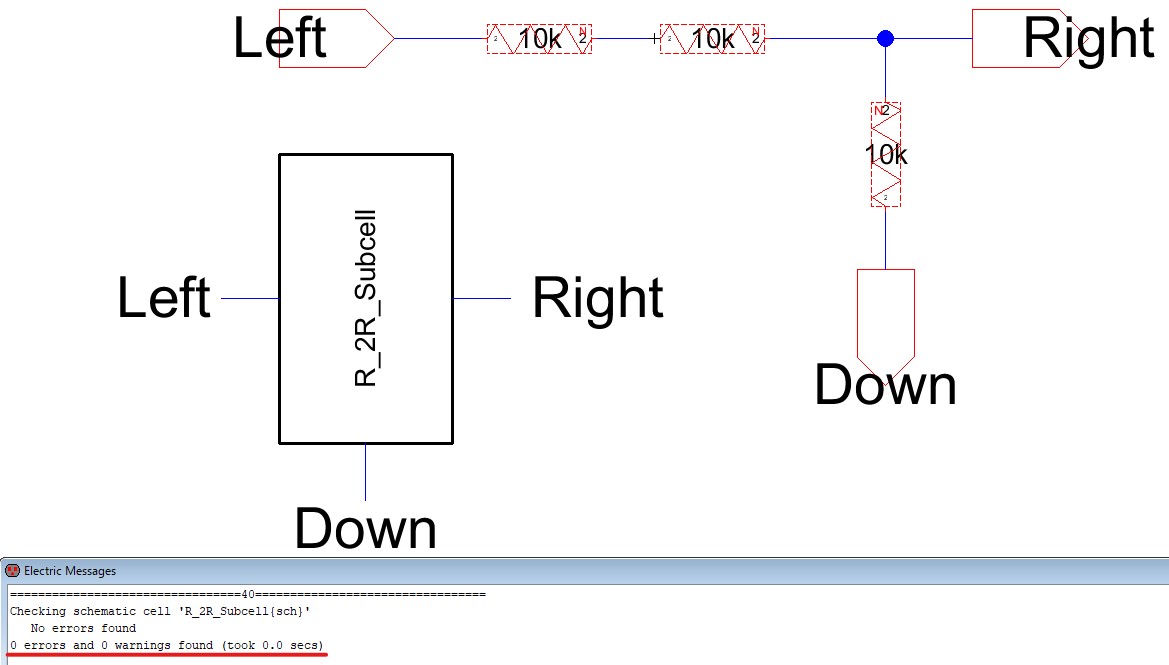
Figure 1. Subcell of the repeating structure with icon and clean DRC check.
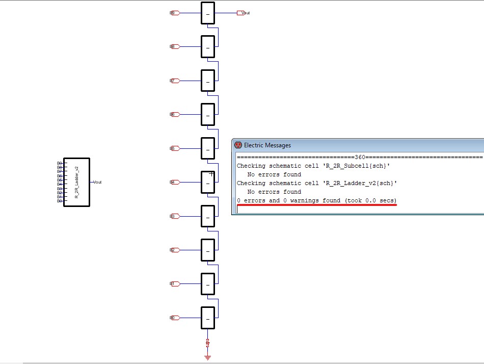
Figure 2. R-2R DAC using subcell icon to replace the repeating structure with icon and clean DRC check.
Task 2:
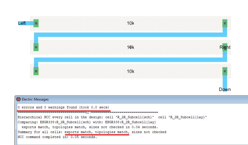
In task 2, we had to create the layout of the subcells for the R-2R ladder. To begin we had to create the layout view for the 'R_2R_Subcell', as shown in Figure 3,
by making three 10k resistors using a width of 15 and a length of
187.5. After the layout was created, we needed to create the layout for
the 'R_2R_Ladder_v2'
so we used the subcell we just created and created a 10-cell column
with a spacing of 75 Lambda, as shown in Figure 4. Once we had a clean
DRC, we were able to wire everything and run a DRC and NCC check, as
shown in Figure 5. After we replaced the DAC from the previous lab and
inserted our 'R_2R_Ladder_v2' icon, shown in Figure 6, and ran the
simulation in LTSpice, as shown in Figure 7. The results were as
expected as it would work similarly to the DAC.
Figure
3. Created the layout view for the R_2R_Subcell using N-Well Resistors
and displaying the results from the DRC and NCC checks.
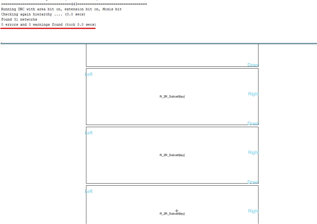
Figure 4. 10-cell column using the 'R_2R_Subcell' with a spacing of 75 Lambda providing the results from the DRC check.
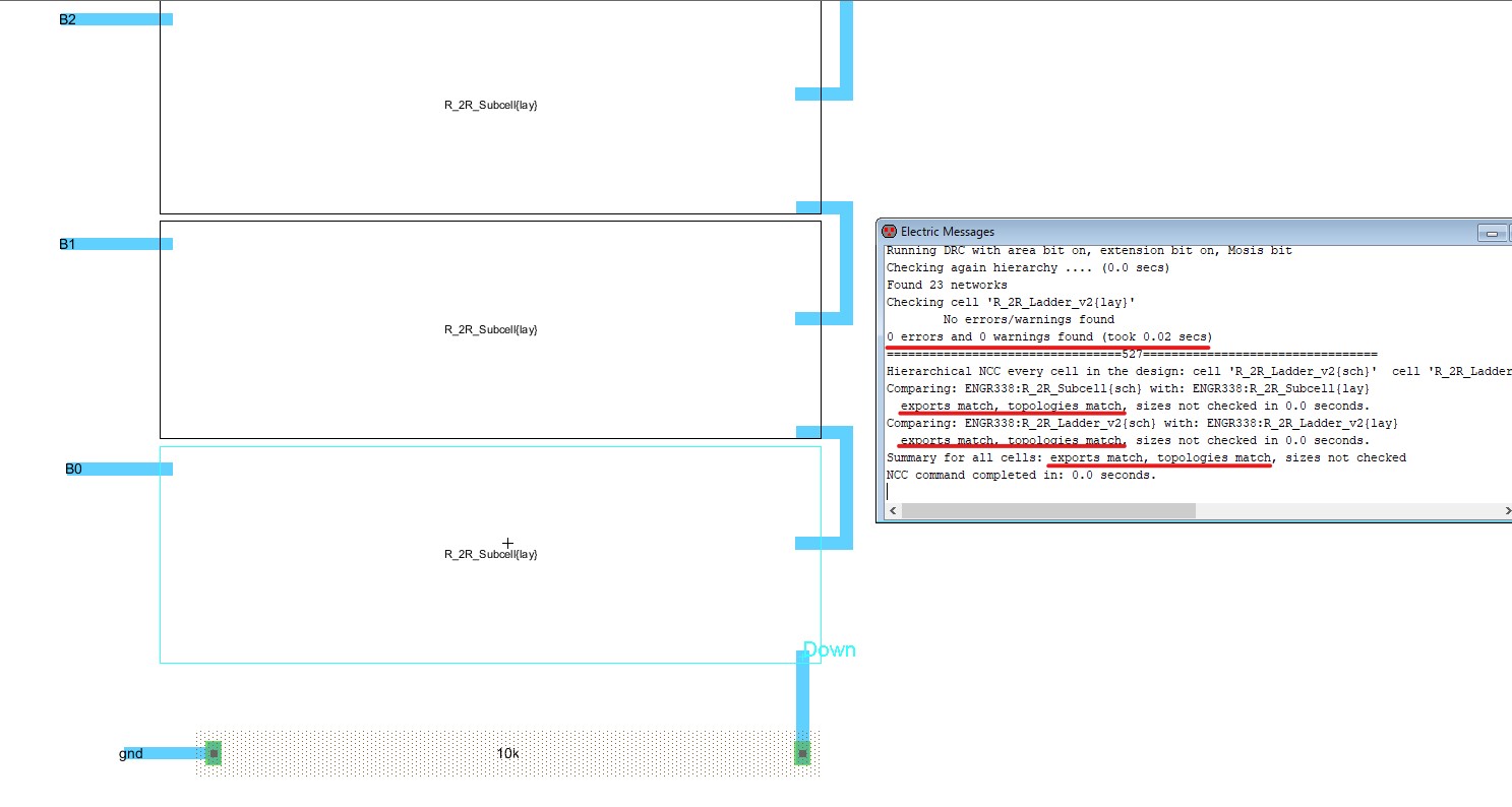
Figure 5. Making all the connections for the 'R_2R_Ladder_v2' and providing the results from the DRC and NCC checks.
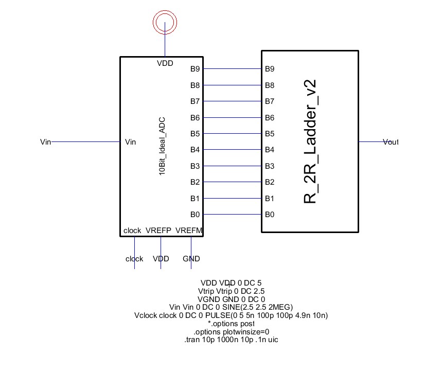
Figure 6. Replaced the DAC from the previous lab and inserted our 'R_2R_Ladder_v2' icon.
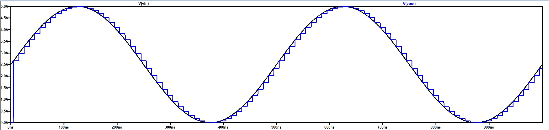
Figure 7. Simulation results in LTSpice of replacing the DAC with the 'R_2R_Ladder_v2'.
Discussion:
By compleing this lab were were able to gain more experience with ElectriVLSI, understand the importance of subcells, created
the layout for the R-2R DAC using N-Well resistors, and became more
familiar with ElectriVLSI and LTSpice for IC design. I felt that this
lab was helpful to learn more about subcells, creating layouts, and
calculating the dimensions of the N-Well Resistor. I am becoming more
comfortable with ElectriVLSI and hope that these skills will come in
hand in the future.
.................................