ENGR 338 2021 Spring
Lab 2: Design an R-2R DAC
Taylor Nakai
tsnakai@fortlewis.edu
Introduction:
In
this lab, we used ElectiVLSI to help to understand an ideal ADC and
DAC, designed a R-2R DAC to replace the ideal DAC given to us, and gain
a familiarity with using ElectiVLSI and LTSpice for integrated circuit
design.
Task 1:
In
Task 1, we needed to copy the ideal ADC-DAC files to our ENGR338
library. Once the files were copied we ran the simulation for the
sim_ADC_DAC{sch} and produced the output as shown in Figure 1.
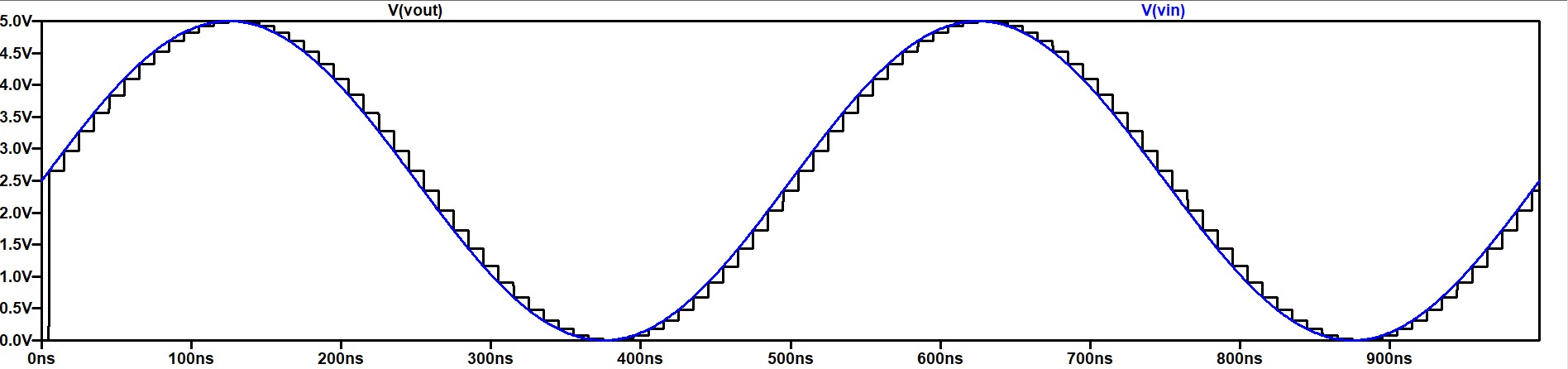
Figure 1. Simulation results from running the sim_ADC_DAC{sch} using LTSpice.
Task 2:
In
Task 2, we needed to build the scematic for the R-2R DAC and run a
simulation using LTSpice. To begin we had to create a R-2R Ladder
schematic and the DRC for the schematic should be clean of errors as
shown in Figure 2. Once the icon had been formatted to our liking we
replaced the original ideal DAC with the R-2R Ladder that we had just
created. After all the proper connections had been made, shown in
Figure 3, a simulation was ran to verify that it produces very similar
results as the ideal one, as can be seen in Figure 4.
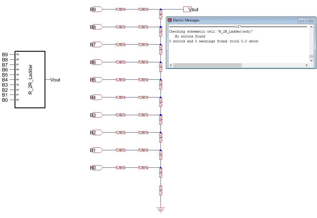
Figure 2. Created R-2R Ladder with icon and DRC showing no errors.
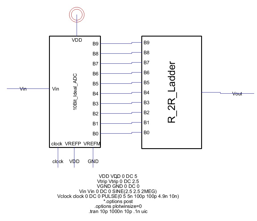
Figure 3. Replace original ideal DAC with the R-2R Ladder that we had just created.
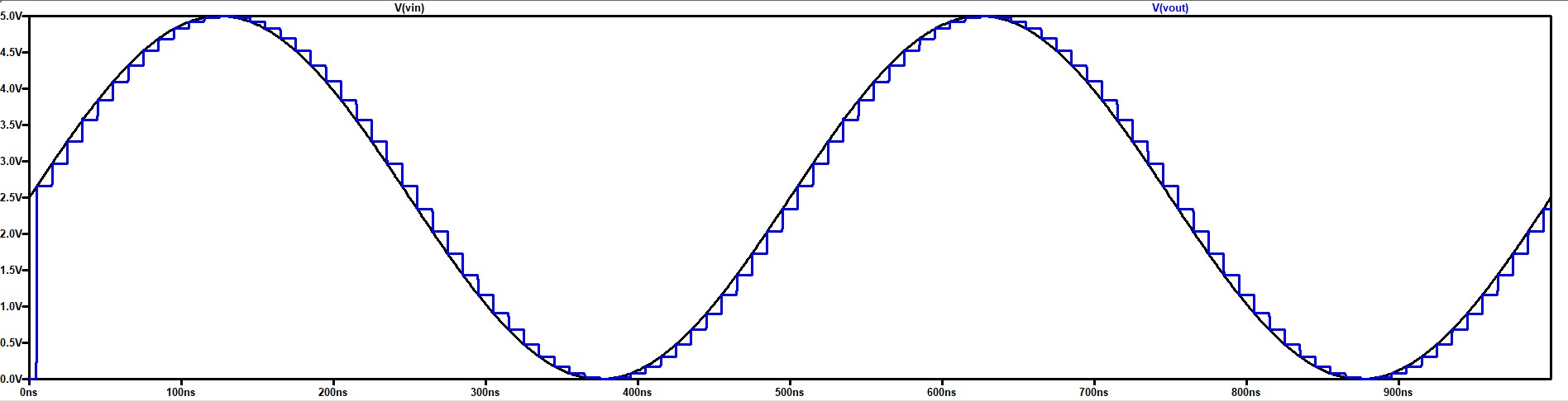
Figure 4. Simulation results from replacing the original ideal DAC with the R-2R Ladder.
Task 3:
In
task 3, we had to test the time delay from the B9 pin when the DAC had
a 10 pF load. We had to ground pins B0-B8, leaving B9 connected to a
pulse, and added a 10 pF load to the output. We had to calculate the
expected time delay using the 0.7RC equation, which the expected time
delay was 70ns. Then we were able to run the simulation using LTSpice
to check if the time delay we calculated matched the simulation, as
seen in Figure 6.
td = 0.7 * R * C
td = 0.7 * 10k * 10p
td = 70 ns
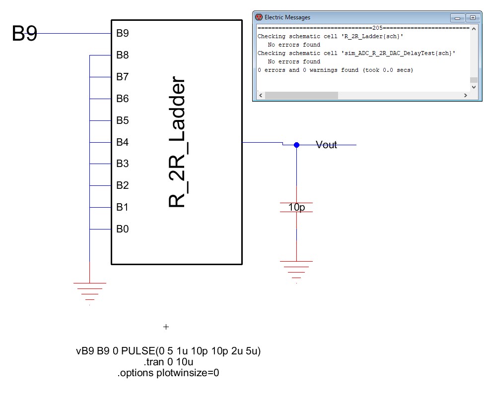
Figure 5. Connection of the R-2R Ladder grounding pins B0-B8, connecting a pulse to B9, and adding a 10pF capacitor.
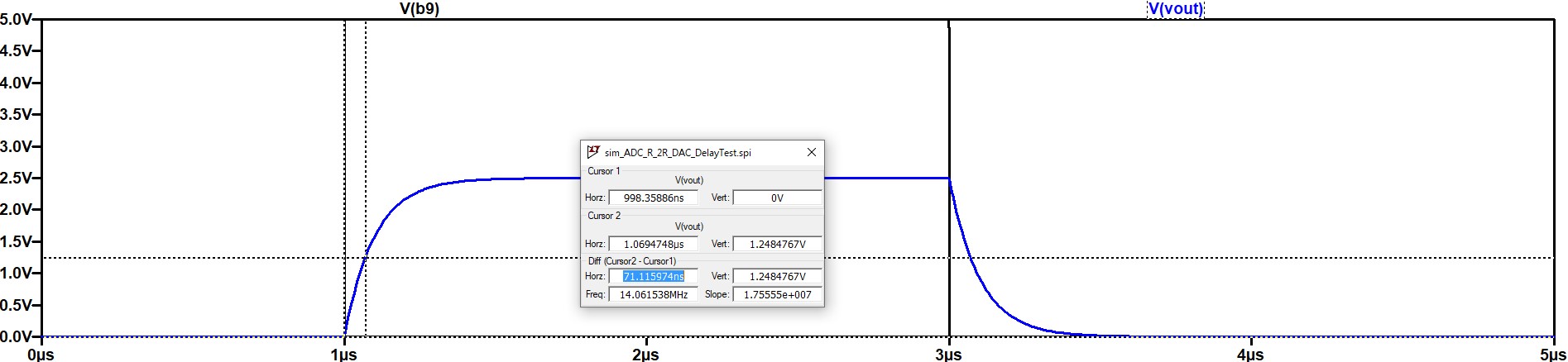
Figure 6. Simulation results from testing the time delay from the B9 pin when the DAC has a 10pF load.
Discussion:
By
completing this lab we were able to gain a familiarity using
ElectriVLSI, have a better understanding of the operation of the ideal
DAC, and designed a R-2R DAC. I felt that this lab helped have a basic
understanding of using ElectriVLSI to prepare me for labs ahead.