CE 433 Spring 2022 Lab 3: More about FPGA - Seven Segment Display and Others Taylor Nakai tsnakai@fortlewis.edu
Introduction: In
this lab, we were tasked with using verilog and vivado to create an
inverter, a 2-bit full adder, an 8-input AND gate, and a 4-1 MUX and
running simulations and using on board verification to
verify the logic. We also were tasked with designing a running LED
program on the FPGA board using 4 LEDs, using the switches to show
numbers 0-9 on the 4 7-segment display, and disable any of the 3
7-segment displays and only show the number on one of the displays.
Completing these tasks will allow us to be more comfortable with using
verilog, vivado, and the 7-segment display.
Task 1: In
this task, we were tasked with using verilog and vivado to demonstrate
the combinational logic blocks in simulation and on board verification
of an inverter, an 2-bit full adder, an 8-input AND gate, and a 4-1
MUX. The inverter verilog code and simulation results are shown in
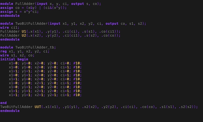
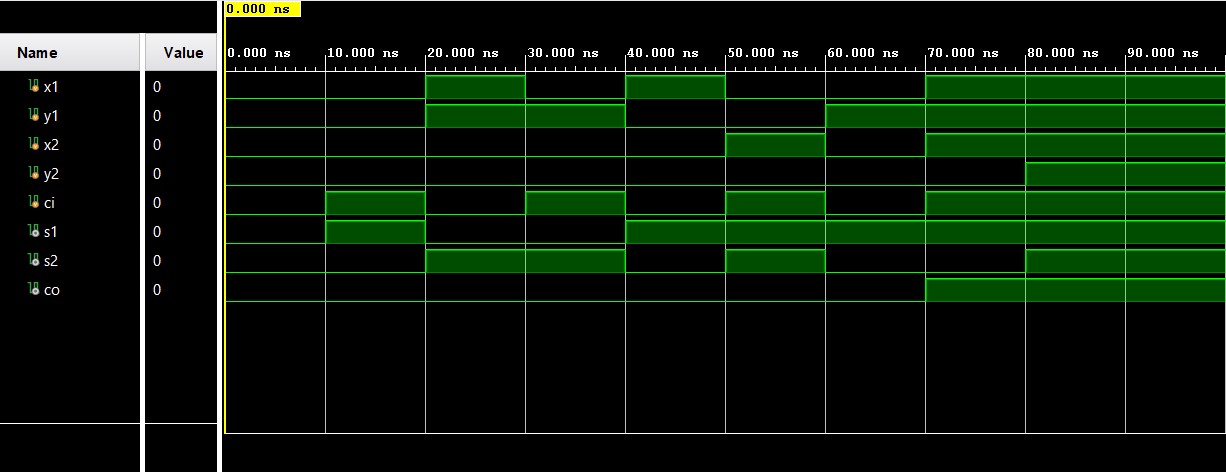
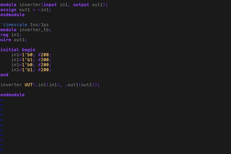
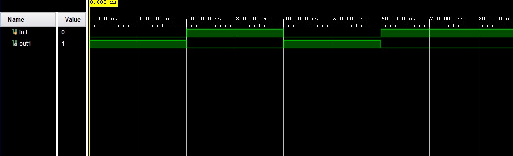
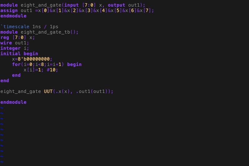
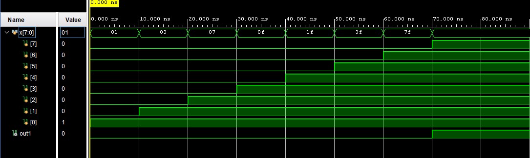
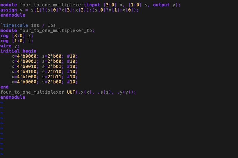
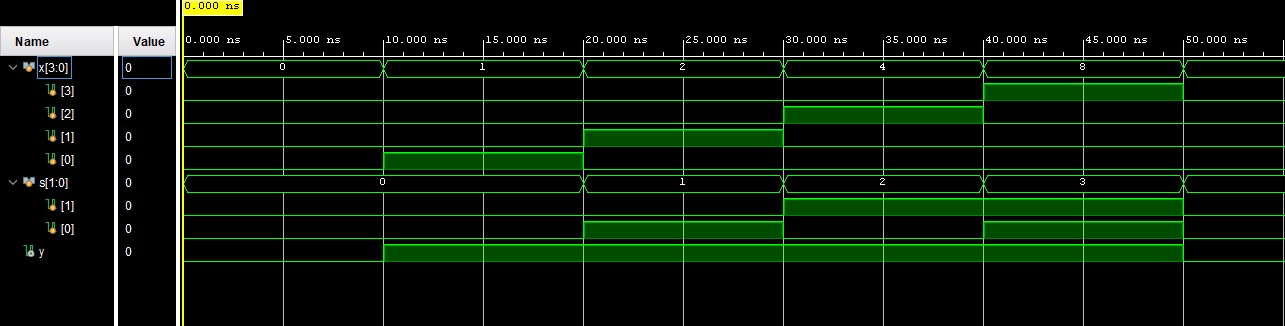
Figure 1. The on board verification is shown in Figure 2. The 2-bit full adder verilog code and simulation results are shown in Figure 3. The on board verification is shown in Figure 4. The 8-input AND gate verilog code and simulation results are shown in Figure 5. The on board verification is shown in Figure 6. The 4-1 MUX verilog code and simulation results are shown in Figure 7. The on board verification is shown in Figure 8. Inverter
Figure 1. Inverter code implemented with vivado simulation results.
Figure 2. Demonstration of the inverter on the Basys 3 Board.
2-Bit Full Adder
Figure 3. 2-bit full adder code implemented with vivado simulation results.
Figure 4. Demonstration of the 2-bit full adder on the Basys 3 Board. 8-Input AND Gate
Figure 5. 8-input AND gate code implemented with vivado simulation results.
Figure 6. Demonstration of the 8-input AND gate on the Basys 3 Board.
4-1 MUX
Figure 7. 4-1 MUX code implemented with vivado simulation results.
Figure 8. Demonstration of the 4-1 MUX on the Basys 3 Board.
Task 2: In
this task, we were tasked with designing a running LED program on the
Basys 3 board that uses 4 LEDs and turns on each of them for 1 second
one-by-one. We
also implemented a 'reset' functino to reset the LEDs to the original
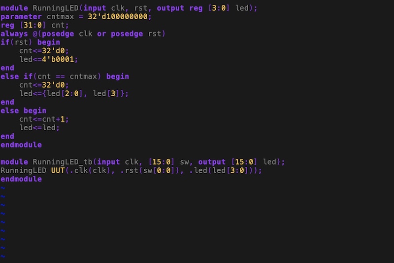
state by switching on sw[0]. The running LED verilog code is shown in
Figure 9. The on board verification is shown in Figure 10. Figure 9. Running LED code to be used on the Basys 3.
Figure 10. Demonstration showing the 'Running LED' code on the Basys 3. Task 3: In
this task, we were tasked with interfacing the switches with the 4
7-segment display on the board. We wanted to be able to display numbers
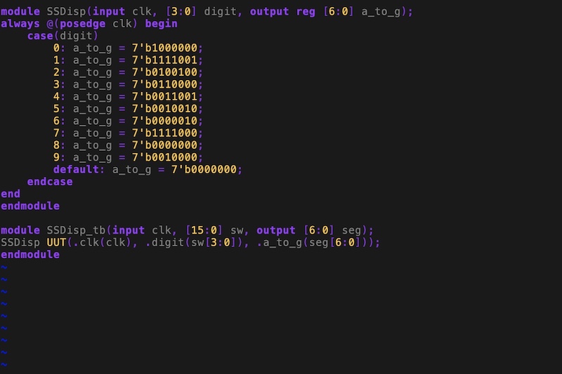
0-9. The verilog code is shown in Figure 11. The on board verification is shown in Figure 12.
Figure 11. Using switches to display numbers 0-9 on 4 7-segment display code to be used on the Basys 3.
Figure 12. Demonstration showing the 'SSDisp' code on the Basys 3.
Task 4: In this task,we
were tasked with modifying Task 3 where we interfaced the switches with the 4 7-segment display
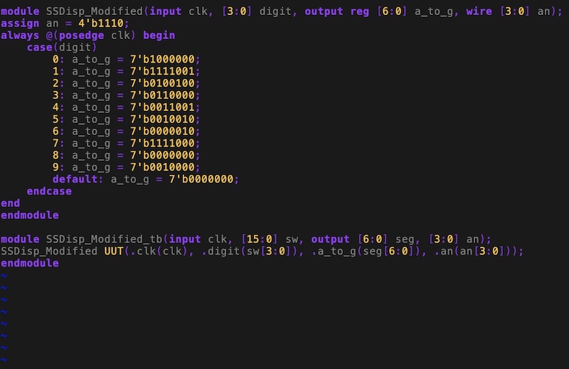
on the board to disable 3 of the 7-segment displays and only display numbers 0-9 only one of the displays. The verilog code is shown in Figure 13. The on board verification is shown in Figure 14.
Figure 13. Using switches to display numbers 0-9 on 1 7-segment display code to be used on the Basys 3.
Figure 14. Demonstration showing the 'SSDisp_Modified' code on the Basys 3.
Discussion: By
completing this lab, we were able to gain more comfortability working
with verilog, vivado, and FPGA's. We were able to to gain more
experience creating combinational logic blocks, on board verification,
using the on-board oscillator, and using the 7-segment display. I think
this was a great introduction into using the 7-segment display. I
believe that these skills will be useful in the future. Overall, this lab was interesting and I can't wait to learn more. ................................................................................................