CE 433 Spring 2022
Sequential Circuit Tutorial
Taylor Nakai
tsnakai@fortlewis.edu
Introduction:
In
this homework, we were given the tasks of determining the logic
equations from a state table, drawing sequential circuits, implementing
sequence detectors in verilog using two methods, implemeting four
different types of shift registers, building a conter module, and
finding the logic equations of a circuit and implementing in verilog.
Task 1:
In
task 1, we were given the task of using the state table given to
determine the logic equations for q1(n+1) and y. Once the logic
equations were found we were able to draw the sequential circuit for
q1(n+1) and y. Figure 1 shows both the logic equations and the
sequential circuit.
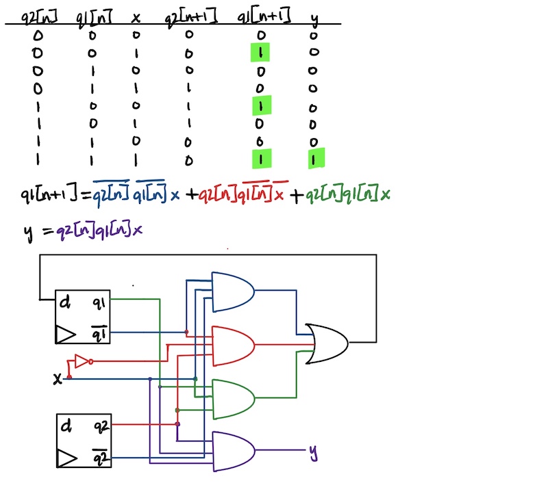
Figure 1. The logic equations and sequential circuit for the state table give.
Task 2:
In
task 2, we were given the task of repeat the work done in section 3 to
implement the sequence detector example in verilog using two methods
(the given method and the behavioral one) in vivado and show the
simulation results. Figure 2 shows the code and simulation
of the first method given. Figure 3 shows the code and simulation of
the second method, which implements a behavioral structure.
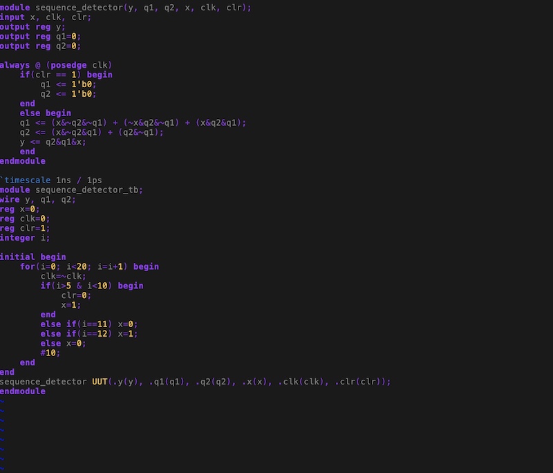
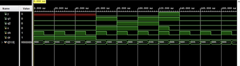
Figure 2. Sequence detector code and simulation in vivado using method given shown.
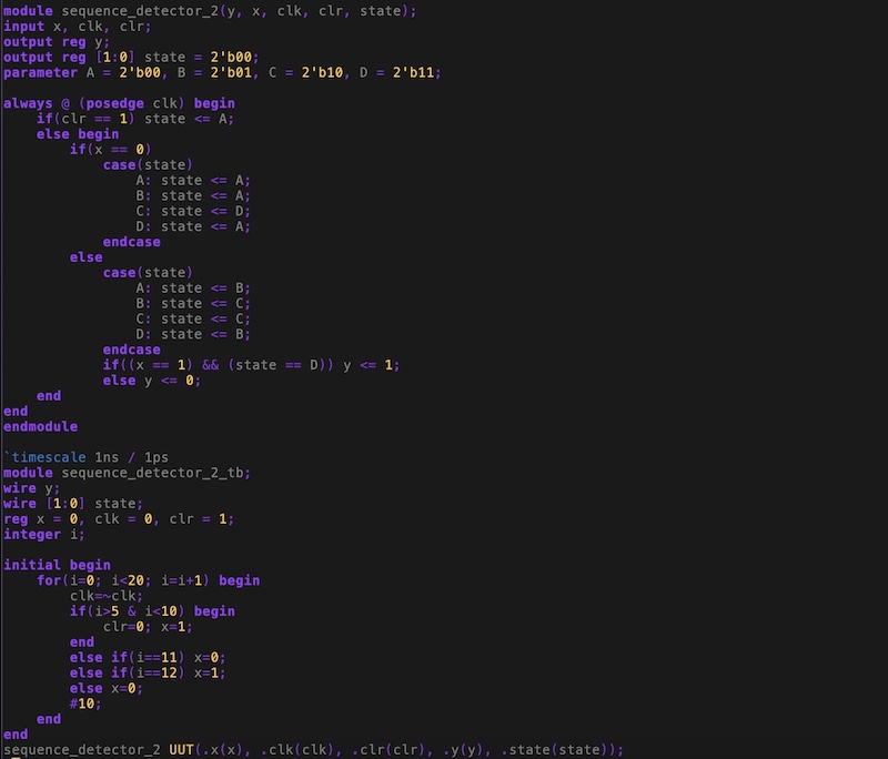
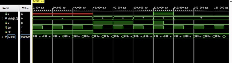
Figure 3. Sequence detector code and simulation in vivado using behavioral method.
Task 3:
In
task 3, we were given the task of simulating four different types of
shift registers. The four different types of shift registers include
the serial in/serial out (SISO), parallel in/serial out (PISO),
parallel in/parallel out (PIPO), and serial in/parallel out (SIPO).
Figure 4 shows the code and simulation of the SISO shift register. Figure 5 shows the code and simulation of the PISO shift register. Figure 6 shows the code and simulation of the PIPO shift register. Figure 7 shows the code and simulation of the SIPO shift register.
SISO Shift Register
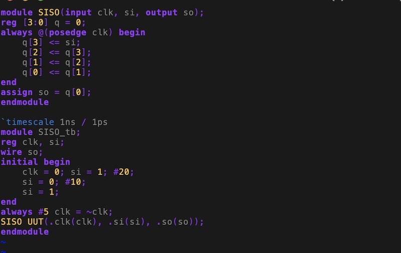
Figure 4. SISO code and simulation in vivado.
PISO Shift Register
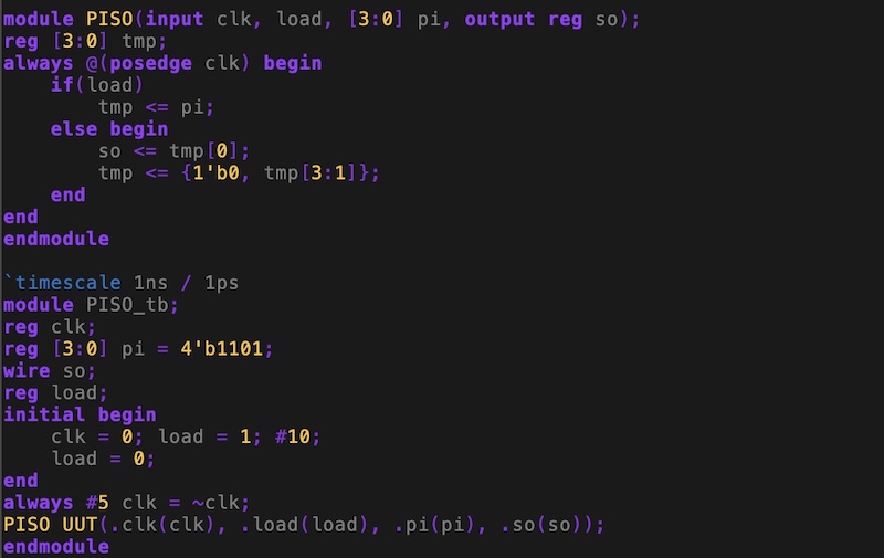
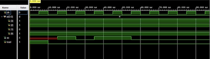
Figure 5. PISO code and simulation in vivado.
PIPO Shift Register
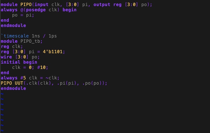
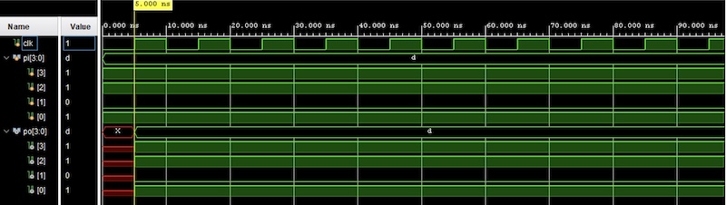
Figure 6. PIPO code and simulation in vivado.
SIPO Shift Register
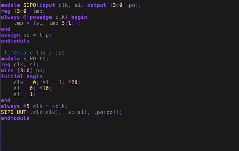
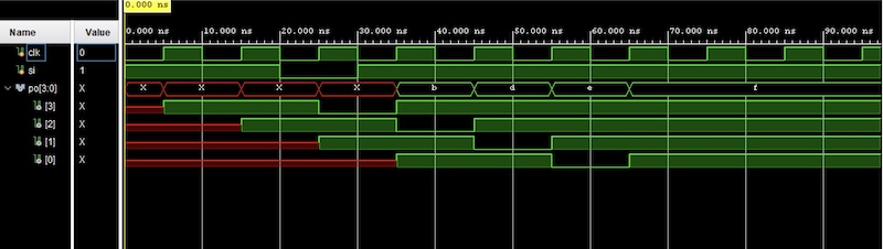
Figure 7. SIPO code and simulation in vivado.
Task 4:
In
task 4, we were given the task of building a counter module and showing
the simulation results. A n-bit synchronous counter was built in
verilog, for testing purposes a two bit synchronous counter was used,
and then simulated to verfify the logic. Figure 8 shows the code and simulation of the two bit synchronous counter.
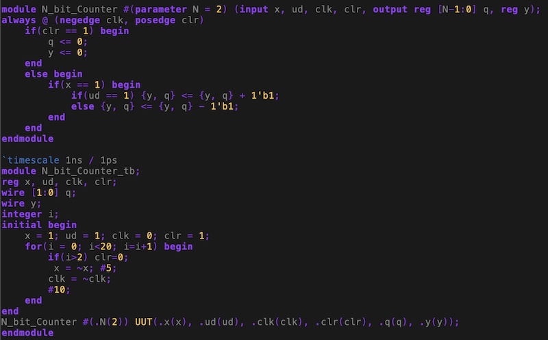
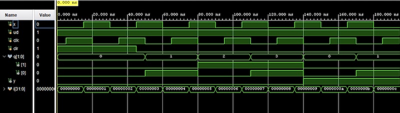
Figure 8. Two bit synchronous counter code and simulation in vivado.
Task 5:
In
task 5, we were given the task of finding the logic equations of the
circuit shown in Figure 9. Once the logic equations were found we were
then tasked with implementing it using verilog and testing it in
vivado. Figure 10 shows the work to find the logic equations. Figure 11
shows the code and simulation results of the circuit.
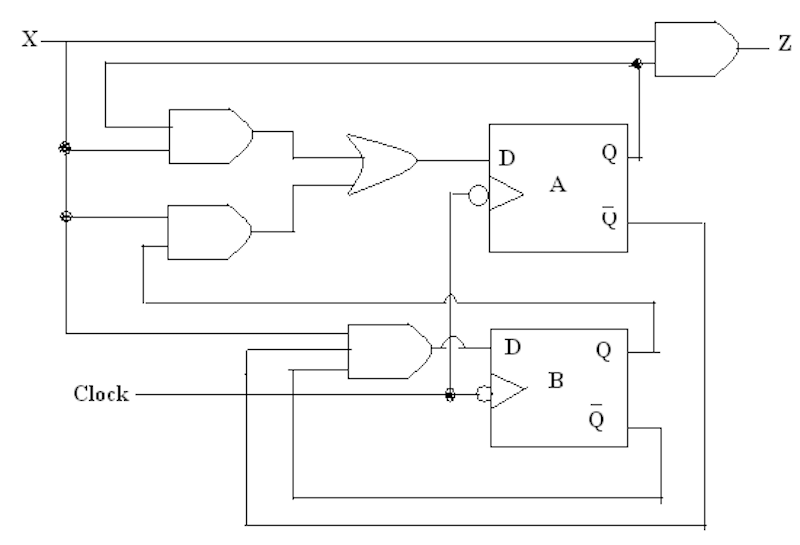
Figure 9 Circuit given to find the logic equations.
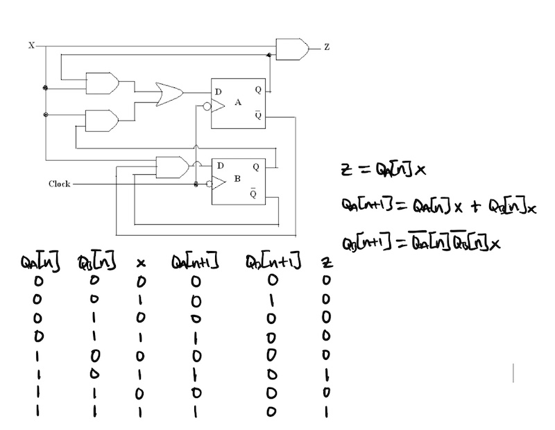
Figure 10. Work done to find the logic equations.
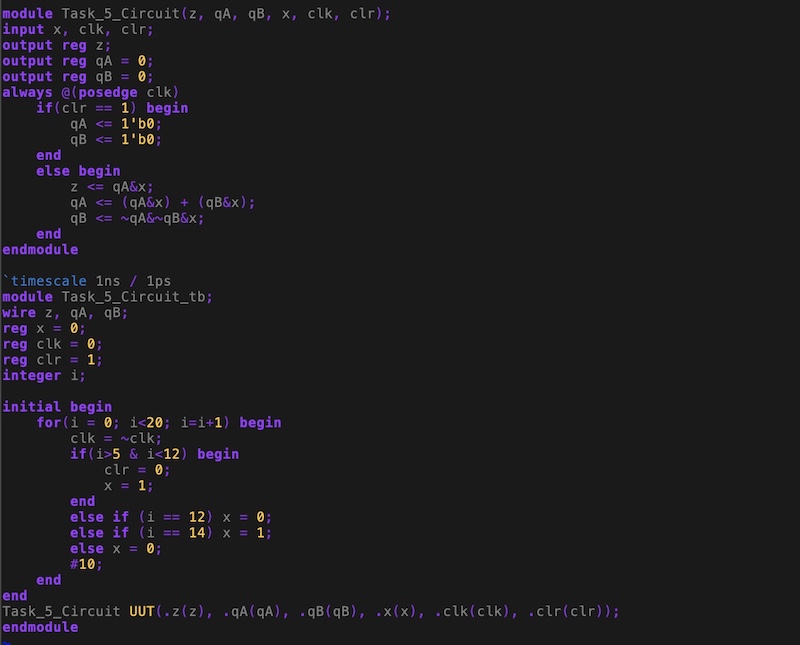
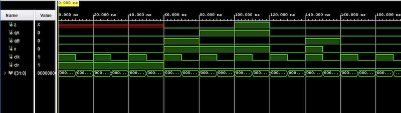
Figure 11. Circuit code and simulation in vivado.
Discussion:
By completing this homwork, it allowed me to be more comfortable with determining
the logic equations from a state table, drawing sequential circuits,
implementing sequence detectors in verilog using two methods,
implemeting four different types of shift registers, building a conter
module, and finding the logic equations of a circuit and implementing
in verilog.
I liked this tutorial as it allowed us to actually use state tables and
circuits. Overall, I think this homework was a really fun one and I
look forward to the next!
............................................................