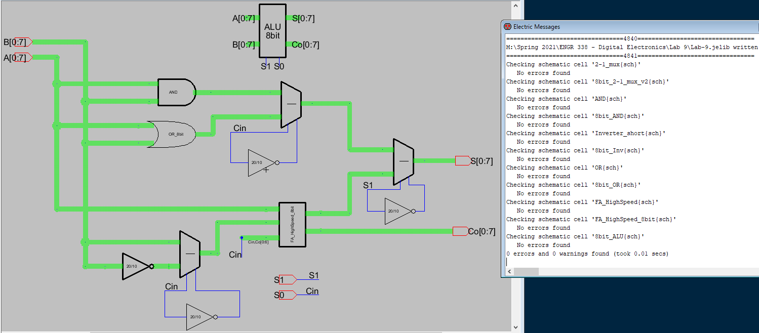
Figure 1. Final 8bit_ALU{sch} design with DRC scan passed!
After
the schematic was complete, three simulations were ran in LTSpice to
further prove that the design was correct and the logic for each
operation worked. The different operations were determined by variables S1 and S0; if
S1S0 = "00" then that would make the ALU operate in AND logic, "01" for
OR logic, "10" for addition, & "11" for subtraction. Variables
S[0:7] will represent the output of A and B depending on the operation.
Co[7] is used in case there's a overflow and it "carries out" that 9th
bit. In the following four figures are demonstrations of each simulation outputting the correct results.
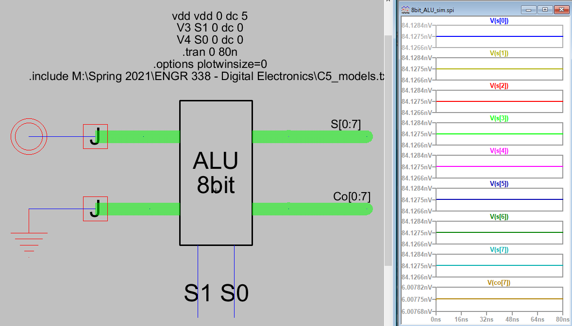
Figure 2. S1S0 = 00 (AND logic), A=1111 1111 AND B=0000 0000 = 0000 0000, Co= 0
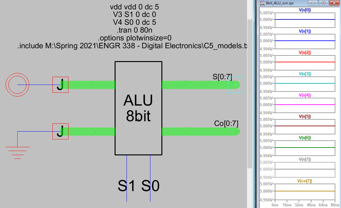
Figure 3. S1S0 = 01 (OR logic), A=1111 1111 OR B=0000 0000 = 1111 1111, Co= 1
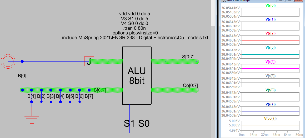
Figure 4. S1S0 = 10 (addition operation), A=1111 1111 + B=0000 0001 = 0000 0000, Co= 1
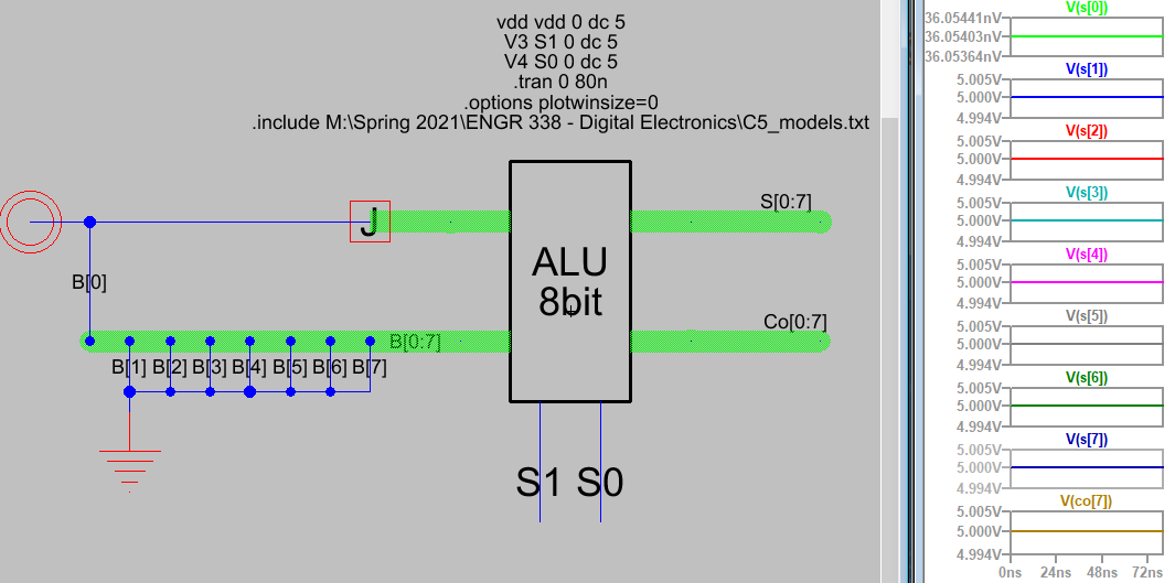
Figure 5. S1S0 = 11 (subtraction operation), A=1111 1111 - B=0000 0000 = 1111 1110, Co= 1
Figure 2. S1S0 = 00 (AND logic), A=1111 1111 AND B=0000 0000 = 0000 0000, Co= 0
Figure 3. S1S0 = 01 (OR logic), A=1111 1111 OR B=0000 0000 = 1111 1111, Co= 1
Figure 4. S1S0 = 10 (addition operation), A=1111 1111 + B=0000 0001 = 0000 0000, Co= 1
Figure 5. S1S0 = 11 (subtraction operation), A=1111 1111 - B=0000 0000 = 1111 1110, Co= 1
Task 2 was when the layout was designed for the 8-bit ALU. This took a lot of time and immense concentration to complete. The overall structure was followed by what was provided in the lab itself.
I made the mistake of importing different designs from previous labs
and had to go through and replace/update almost 6 to 8 designs that I
had already made. Eventually I had successfully created the layout with
it passing the DRC and NCC scans, all of which can be seen below.
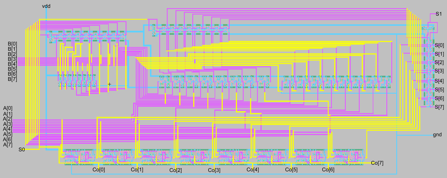
Figure 6. Final 8bit_ALU{layout} design
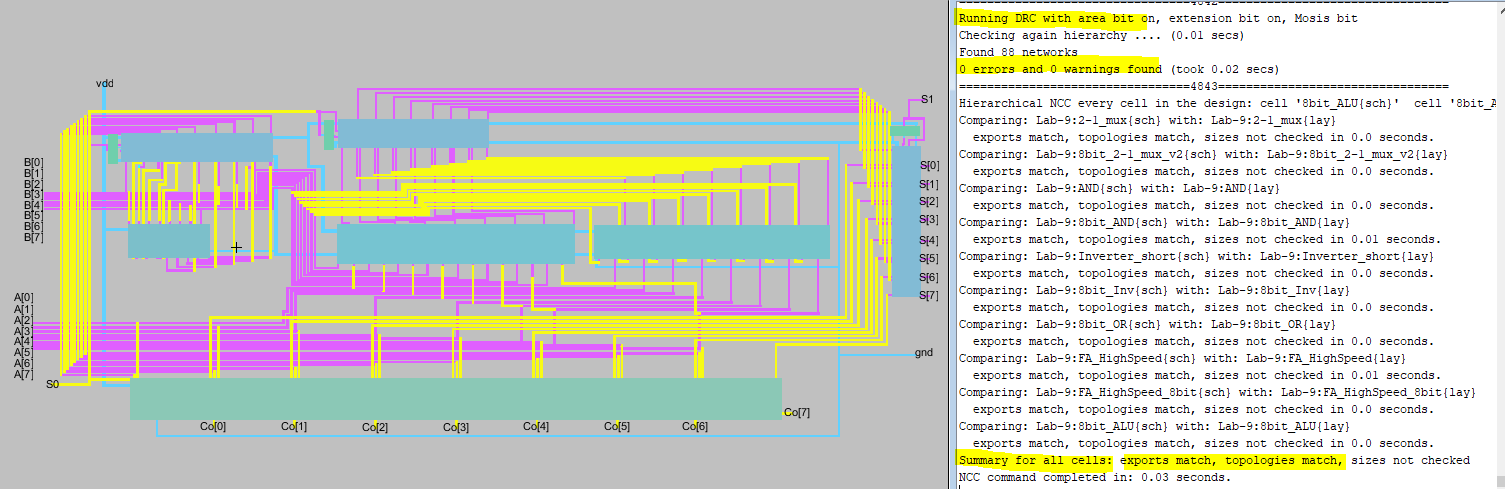
Figure 7. 8bit_ALU{layout} with DRC and NCC scans successfully passed.
Figure 6. Final 8bit_ALU{layout} design
Figure 7. 8bit_ALU{layout} with DRC and NCC scans successfully passed.