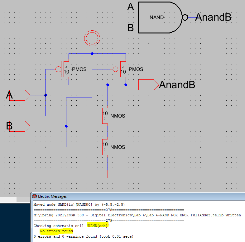
Figure 1. NAND gate schematic + icon with DRC scan passed
A
LTSpice waveform was developed from a simulation ran on the NAND icon
to prove it was correctly developed. The resulting waveform can be seen
in Figure 2.
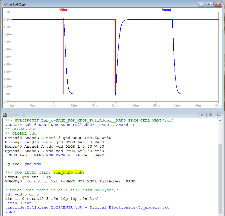
Figure 2. LTSpice waveform of NAND simulation
Figure 2. LTSpice waveform of NAND simulation
After
the simulation, the layout had to pass the DRC and NCC scans in order
to procced to the next task. Thankfully it did and the results can be
seen in Figure 3.
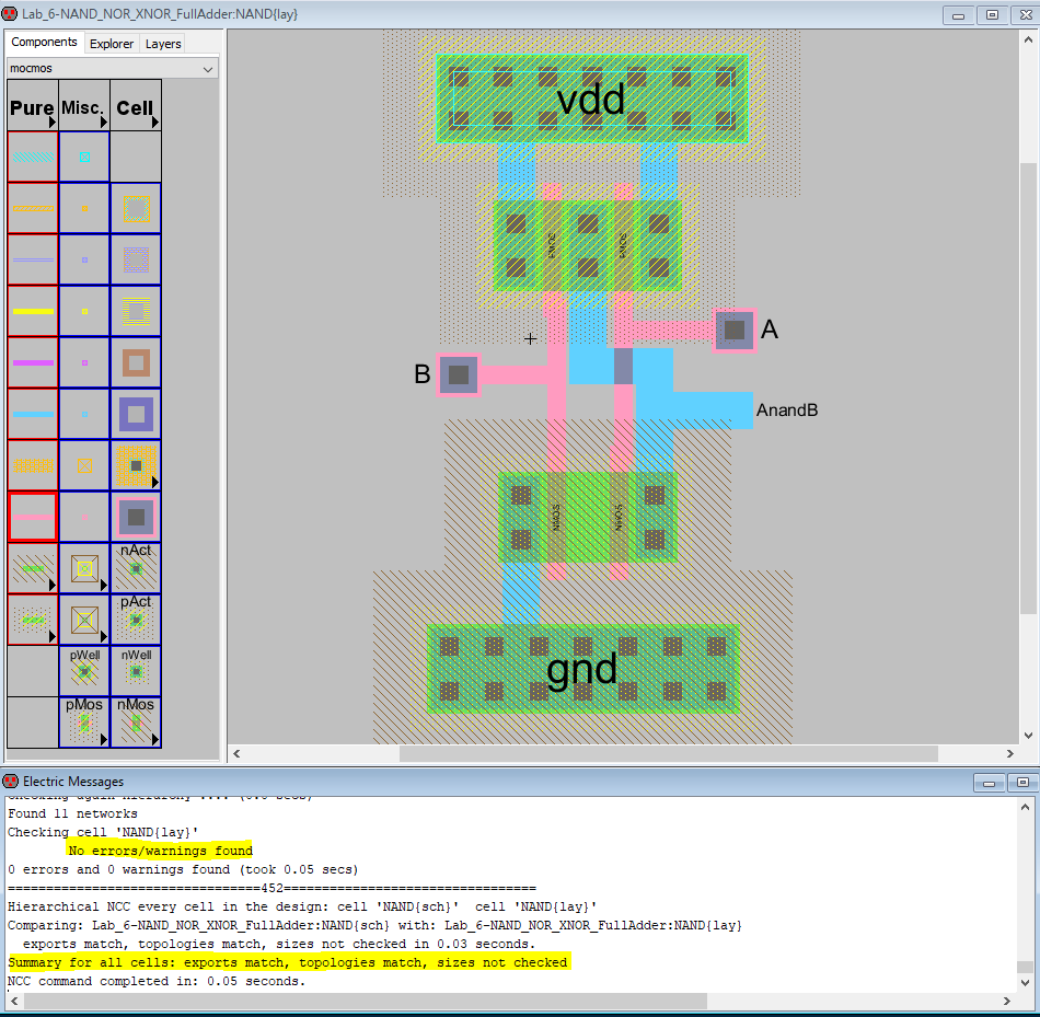
Figure 3. NAND gate layout with DRC + NCC scans passed
Figure 3. NAND gate layout with DRC + NCC scans passed
Task 2 had the exact same process for the NOR gate and that process can
be seen in-order from Figure 4 to Figure 6 below.
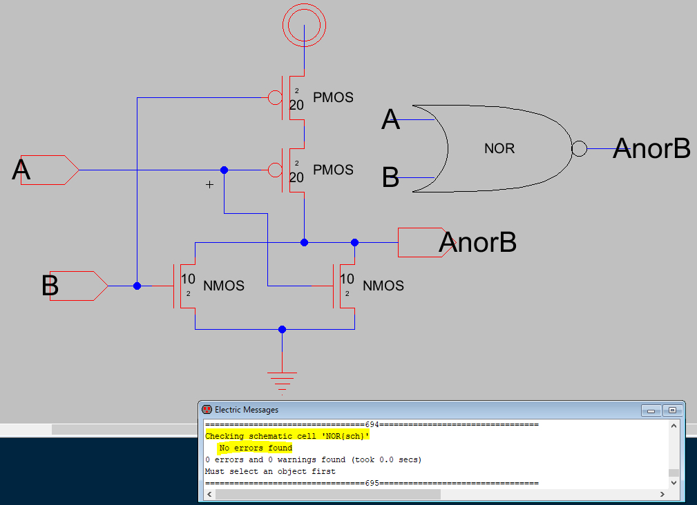
Figure 4. NOR schematic and icon plus DRC scan completed
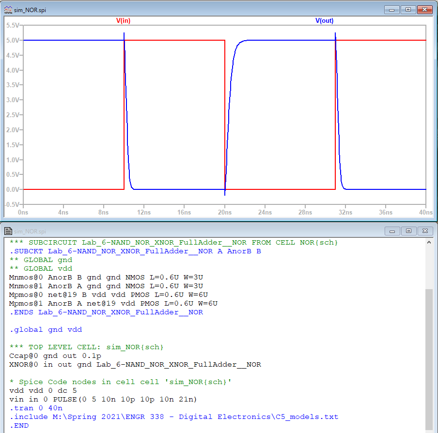
Figure 5. NOR gate simulation in LTSpice
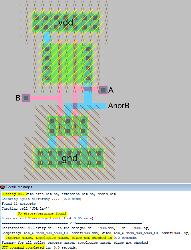
Figure 6. NOR layout with DRC + NCC scans passed
Figure 4. NOR schematic and icon plus DRC scan completed
Figure 5. NOR gate simulation in LTSpice
Figure 6. NOR layout with DRC + NCC scans passed
Task
3 had the same process plus an extra simulation result and stick
diagram. The first three results would be the schematic design and two
simulation results from a 'gnd' and then a 'vdd' connection to the XOR icon. These results can be seen in-order from Figure(s) 7 to 9 below.
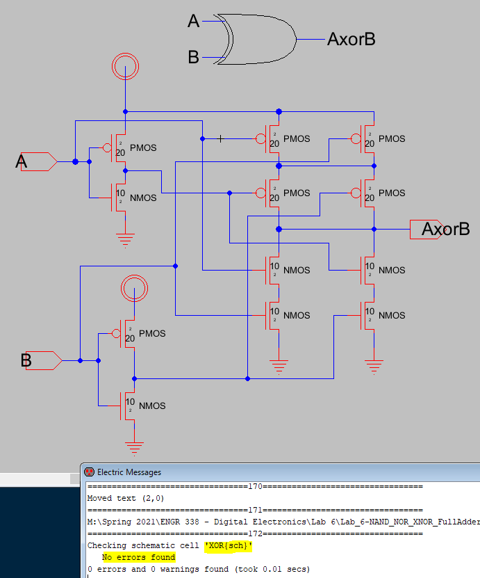
Figure 7. XOR gate schematic plus icon with DRC scan complete
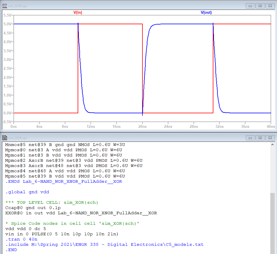
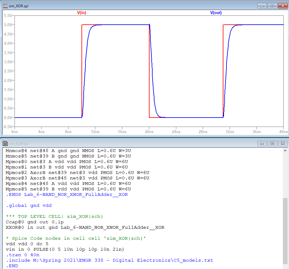
Figure 8. XOR LTSpice waveform with 'gnd' port Figure 9. XOR LTSpice waveform with 'vdd' port
A stick diagram was created before the actual XOR layout and can be seen in Figure 10. Afterwards however, the largest layout so far was created for the XOR gate and can be seen in Figure 11.
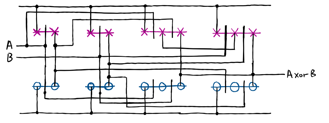
Figure 10. XOR stick diagram with purple PMOS (top) and blue NMOS (bottom)
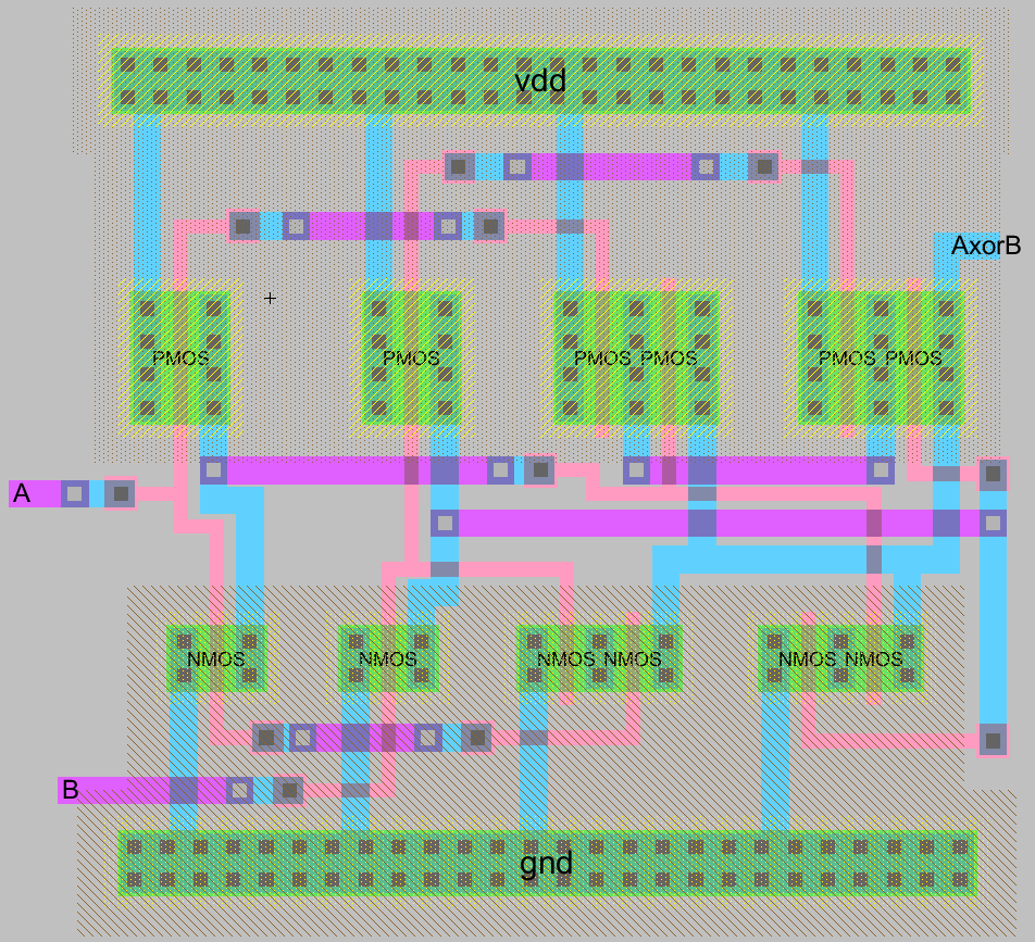
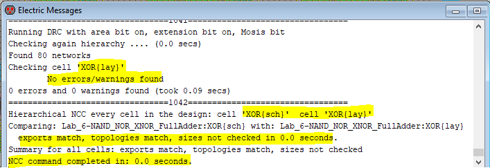
Figure 11. XOR layout with DRC + NCC scans completed
Figure 7. XOR gate schematic plus icon with DRC scan complete
Figure 8. XOR LTSpice waveform with 'gnd' port Figure 9. XOR LTSpice waveform with 'vdd' port
A stick diagram was created before the actual XOR layout and can be seen in Figure 10. Afterwards however, the largest layout so far was created for the XOR gate and can be seen in Figure 11.
Figure 10. XOR stick diagram with purple PMOS (top) and blue NMOS (bottom)
Figure 11. XOR layout with DRC + NCC scans completed
Task 4 had a full-adder (FA) schematic and icon developed and simulated
using both the 'gnd' and 'vdd' connection (similar to the previous
task). Both simulation waveforms can be seen below in Figure(s) 12 and
13.
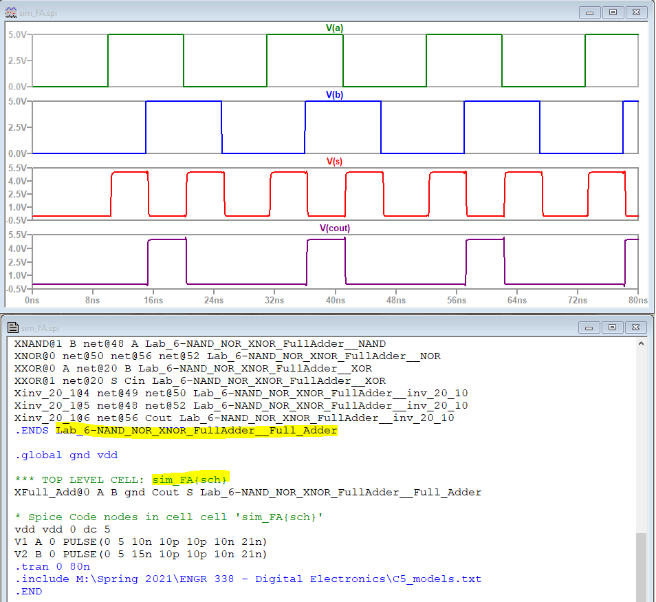
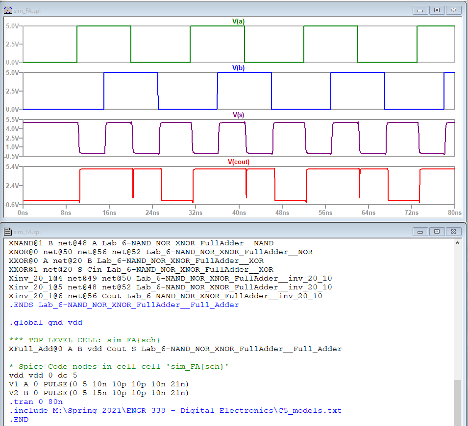
Figure 12. FA LTSpice waveform with 'gnd' port Figure 13. FA LTSpice waveform with 'vdd' port
All previous layouts were then combined to create the FA layout design and was then ran through DRC and NCC scans. The results of all this can be seen in the final Figure 14.
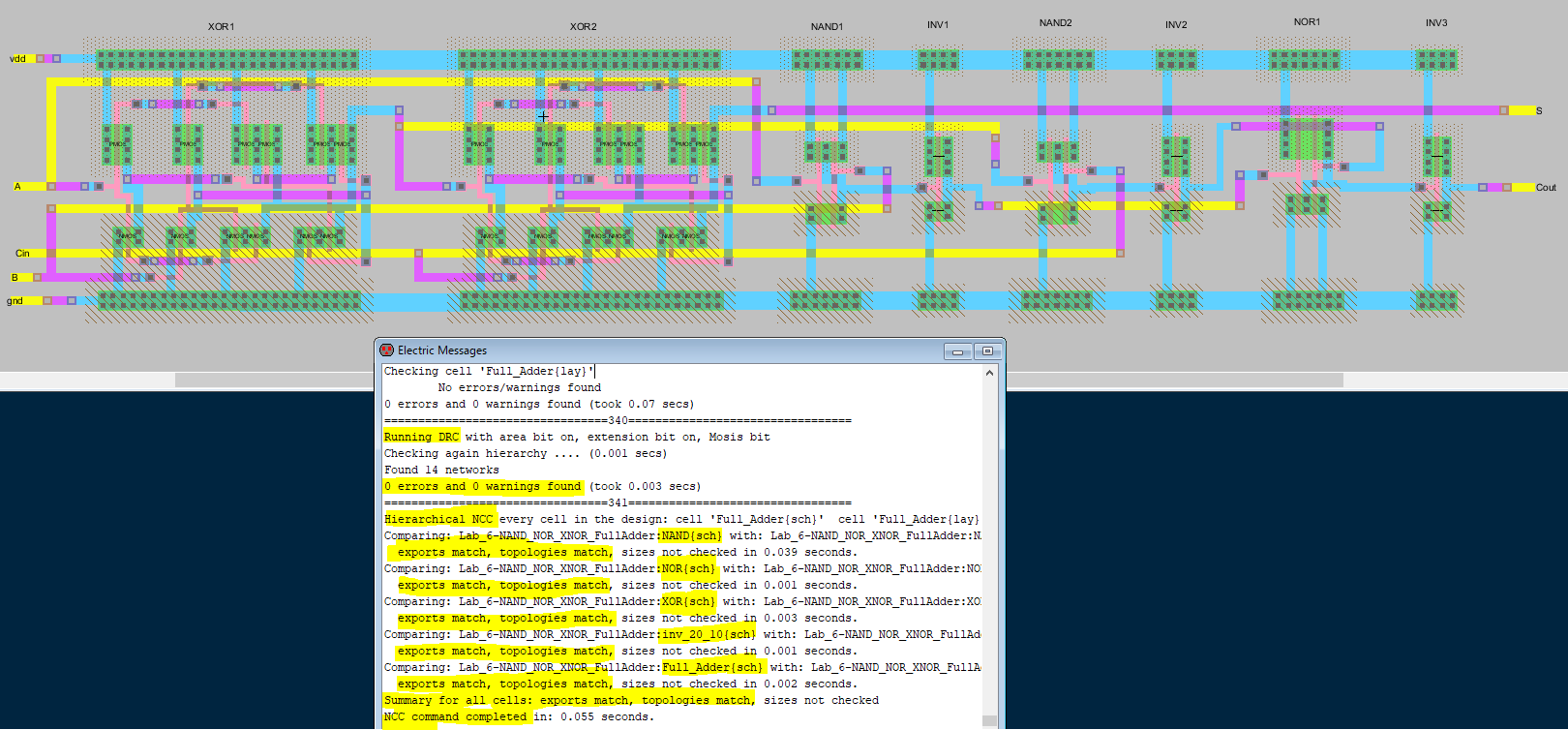
Figure 12. FA LTSpice waveform with 'gnd' port Figure 13. FA LTSpice waveform with 'vdd' port
All previous layouts were then combined to create the FA layout design and was then ran through DRC and NCC scans. The results of all this can be seen in the final Figure 14.
Figure 14. FA layout design with DRC + NCC scans completed for each design used