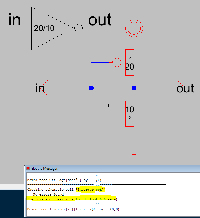
Figure 1. Inverter Schematic Final Design with DRC Scan Passed
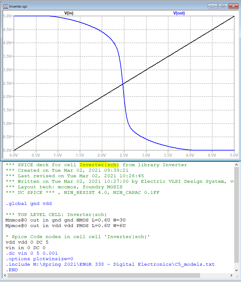
Figure 2. LTSpice Waveform Plot Generated from Inverter Schematic
Once the desired waveform was aquired, the LTSpice code was changed to a PULSE function and simulated. This waveform can be seen in Figure 3 with the new code highlighted.
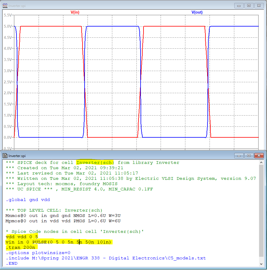
Figure 3. LTSpice PULSE Waveform Generated from Inverter Schematic
Task 2's results contained the new layout for the inverter as well as an LTSpice waveform to prove that the design was correct as well. Figure 4 shows each major result from the final layout design itself (top-left), to the DRC, NCC, and ERC, scans (bottom-left), and the LTSpice waveform data (right-side).
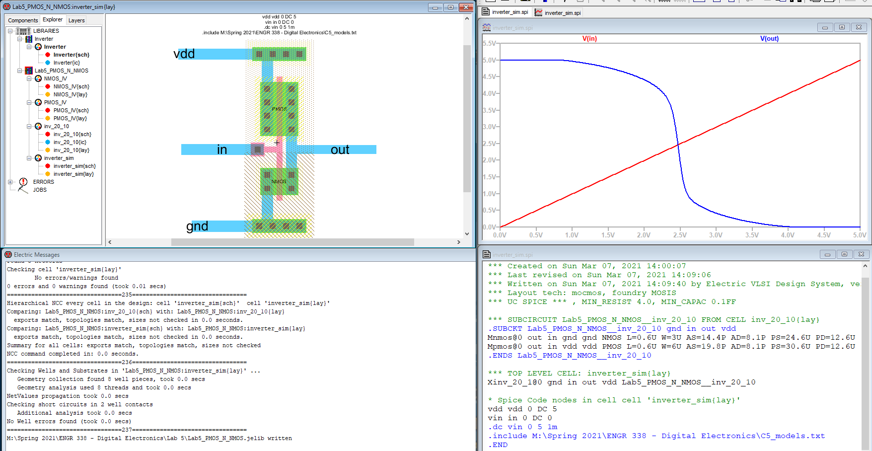
Figure 4. Final Layout Design with Scans and LTSpice Data
Task 3 has additional multipliers to the schematic and layout designs.
The schematic can be seen in Figure 5 where "M=5" and "100/50" were the
new additions.
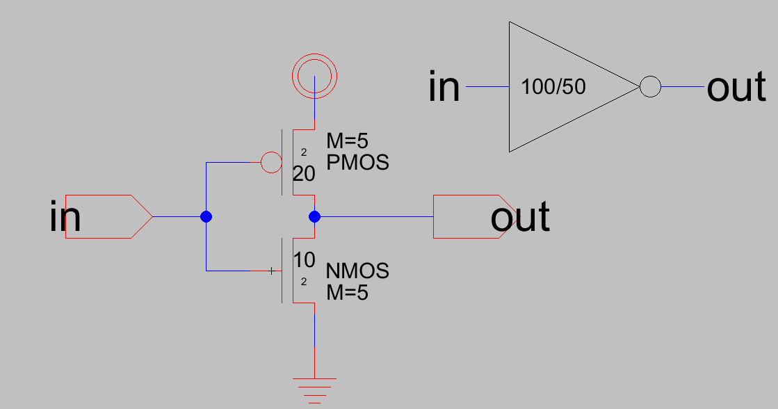
Figure 5. 100/50 Inverter Final Schematic Design
Figure 5. 100/50 Inverter Final Schematic Design
The
layout design has more P/N-transistors and Metal-1 components than the
previous designs. The final layout design can be seen in Figure 6 with
DRC, NCC, and ERC, scans.
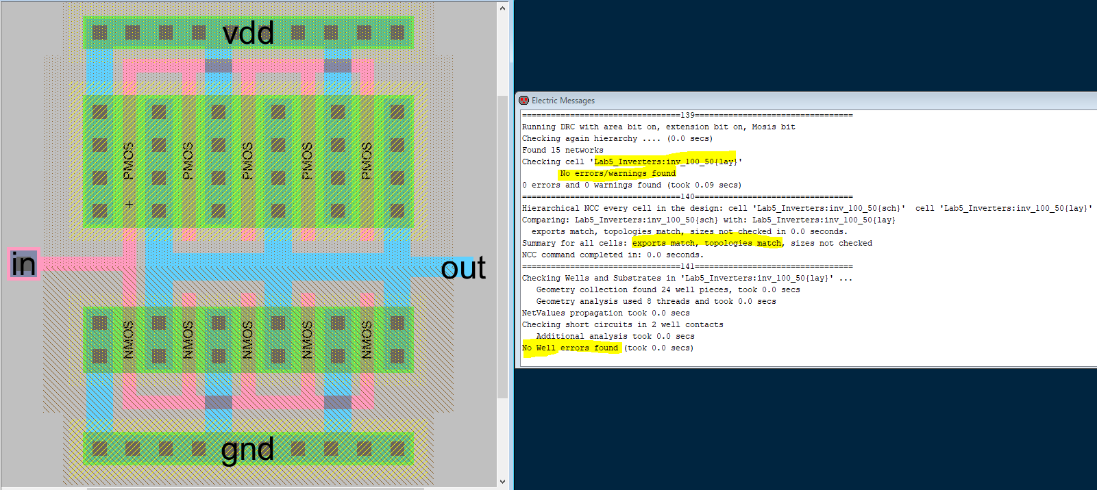
Figure 6. 100/50 Inverter Layout Final Design with Scans Passed
Figure 6. 100/50 Inverter Layout Final Design with Scans Passed
Task 4 has six results, Figures 7 through 12, since both 20/10 and
100/50 inverters were simulated in LTSpice with three different
capacitance values.
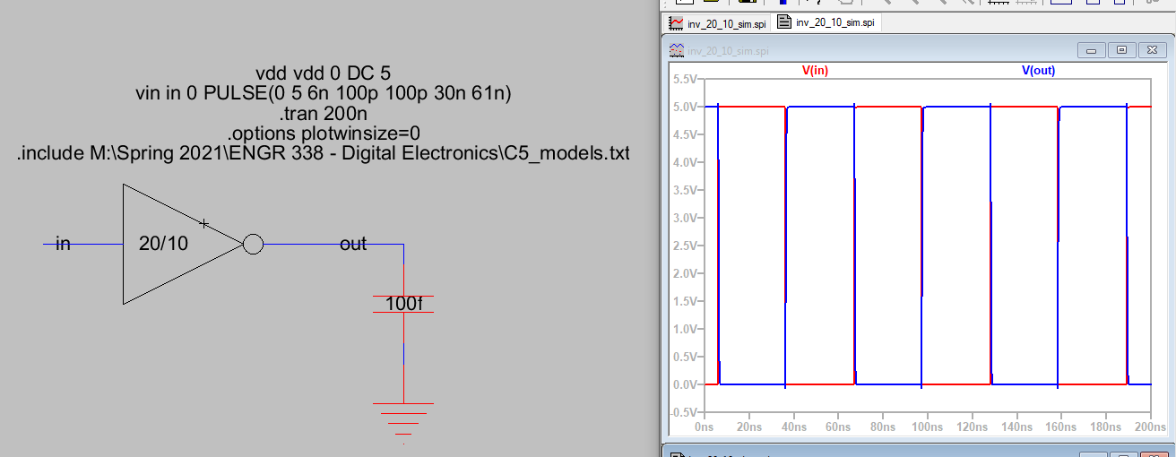
Figure 7. 20/10 Inverter with 100 femto-Farad Capcitor and LTSpice Waveform
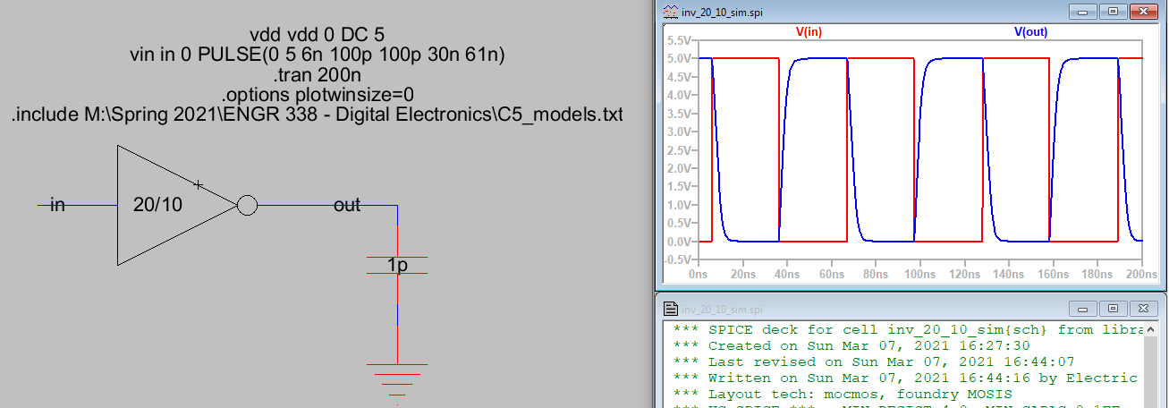
Figure 8. 20/10 Inverter with 1 pico-Farad Capcitor and LTSpice Waveform

Figure 9. 20/10 Inverter with 10 pico-Farad Capcitor and LTSpice Waveform
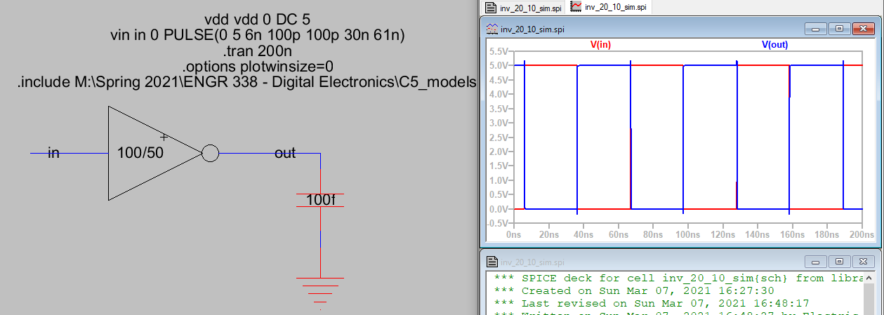
Figure 10. 100/50 Inverter with 100 femto-Farad Capcitor and LTSpice Waveform
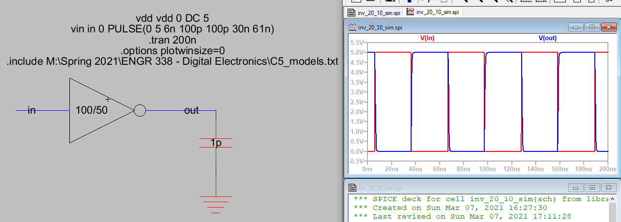
Figure 11. 100/50 Inverter with 1 pico-Farad Capcitor and LTSpice Waveform
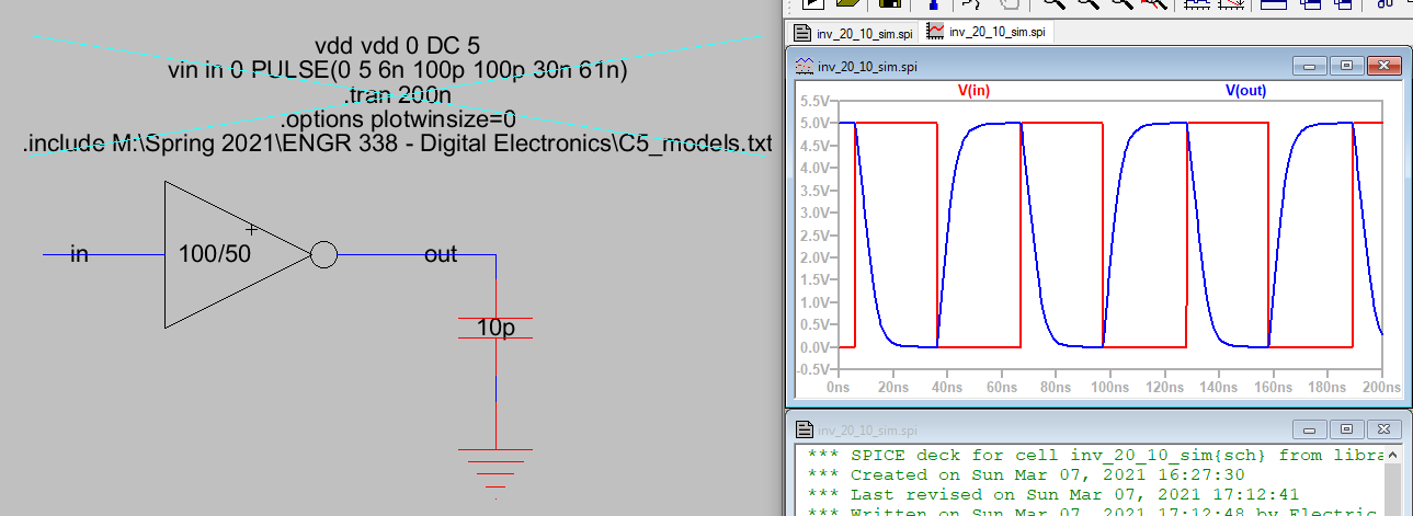
Figure 12. 100/50 Inverter with 10 pico-Farad Capcitor and LTSpice Waveform
Figure 7. 20/10 Inverter with 100 femto-Farad Capcitor and LTSpice Waveform
Figure 8. 20/10 Inverter with 1 pico-Farad Capcitor and LTSpice Waveform
Figure 9. 20/10 Inverter with 10 pico-Farad Capcitor and LTSpice Waveform
Figure 10. 100/50 Inverter with 100 femto-Farad Capcitor and LTSpice Waveform
Figure 11. 100/50 Inverter with 1 pico-Farad Capcitor and LTSpice Waveform
Figure 12. 100/50 Inverter with 10 pico-Farad Capcitor and LTSpice Waveform
Task 5 has two waveforms created from a new design utilizing both of
the inverters, this design can be seen in Figure 13. The new design was
simulated with ALS and IRSIM to create two waveforms, both of these can
be seen in Figure(s) 14 and 15.
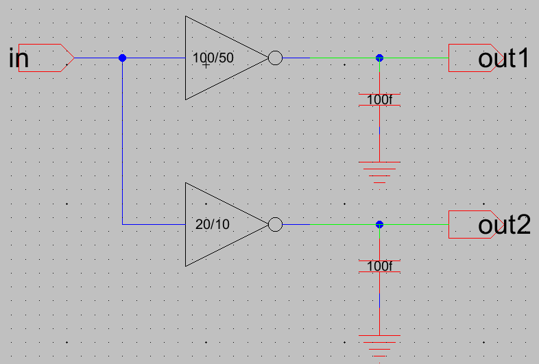
Figure 13. Final Simulation Schematic Design
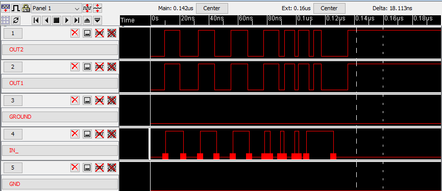
Figure 14. Simulation Waveform from ALS in ElectricVLSI
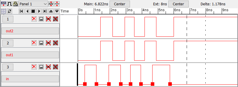
Figure 15. Simulation Waveform from IRSIM in ElectricVLSI
Figure 13. Final Simulation Schematic Design
Figure 14. Simulation Waveform from ALS in ElectricVLSI
Figure 15. Simulation Waveform from IRSIM in ElectricVLSI