ENGR338 Lab 2021 Spring
Lab 4 MOSFETs and IV Curves
Tyrone Bracker
tabrackeryazzie@fortlewis.edu
Lab 4 Report: PMOS and NMOS in ElectricVLSI
Introduction
This lab was about developing and understanding
Metal-Oxide Semiconductors Field Effect Transistors or MOSFETs for
short. The two MOSFETs that were created from this lab were the PMOS
and NMOS. These two had their own schematics and layouts inside of
ElectricVLSI that were plotted via waveforms in LTSpice.
Materials and Methods
The first part was to create a schematic for both the PMOS and NMOS
using components provided by ElectricVLSI. The base was pre-made and
all I had to do was label the bases either "PMOS" or "NMOS" for LTSpice
to reference to later when the waveforms were created. Each pin or
end-segment was also exported to match the 'ground', 'source', and
'drain', points that were appropriate to each transistor.
After the schematics were done, layouts were
developed as well. There were more components when it came to
assembling the PMOS and NMOS layouts; these consisted of "n/pWell"
nodes, "pAct", "metal1-poly1" contacts, etc.. These were resized in
width and combined with exported pins to match the schematics.
LTSpice code was later added to each layout and
schematic to simulate a waveform to make sure each design was correct
in its implementation. PMOS recieved negative voltage values to match
the flow of the current for its transistor while NMOS received positive
values for the same reason. With each new design, NRC, DRC, and ERC,
scans were also run as precautions.
Results
Starting with the NMOS schematic and Layout, Figures 1 and 2 are the
final designs used to form the LTSpice waveform charts. These two can
be seen below.
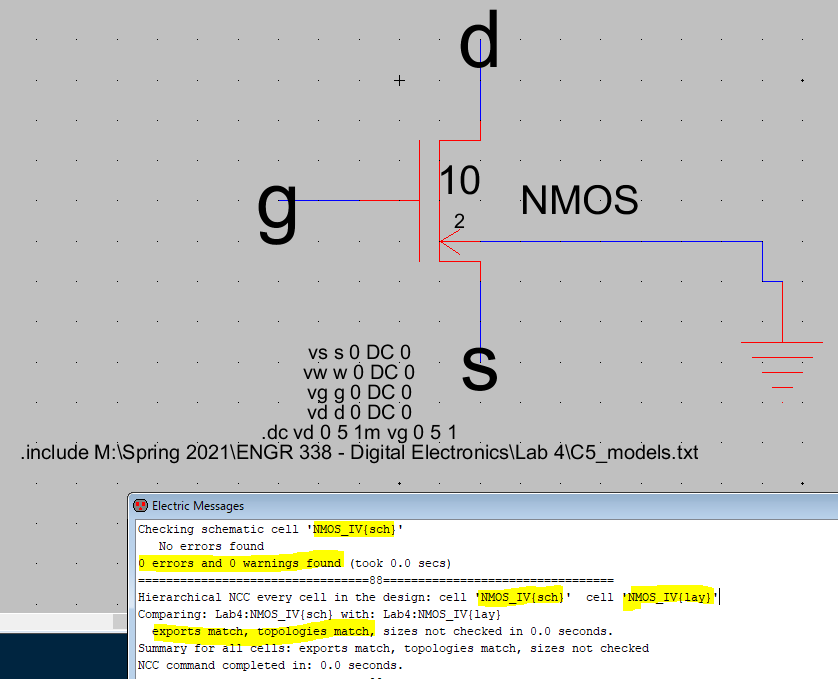
Figure 1. NMOS_IV{sch} final design with LTSpice code and DRC/NRC scans passed
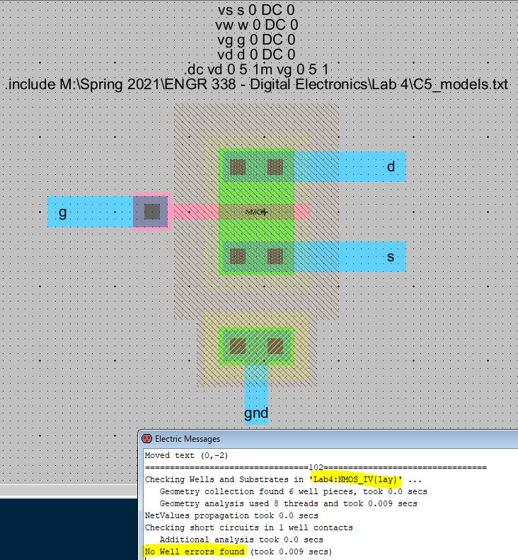
Figure 2. NMOS_IV{lay} final design with LTSpice code and ERC scan passed
Both of these designs were ran and simulated a waveform in LTSpice for
us to see the various outcomes. The results from both NMOS designs can
be seen below in Figures 3 and 4.
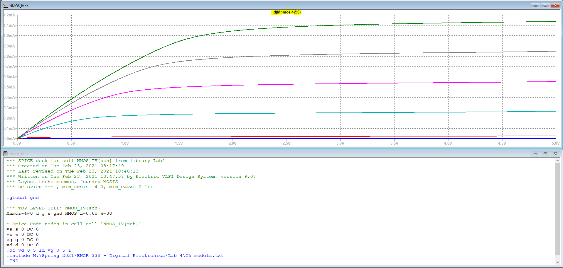
Figure 3. NMOS_IV{sch} LTSpice waveform results from "Id" probed
A quick side-note, for what ever reason, the waveform would display
upside down if "Is" (source current) was probed instead of "Id" (drain
current). This is irregular because every other waveform created by the
other NMOS and PMOS designs all had appropriate orientations when
probing "Is".
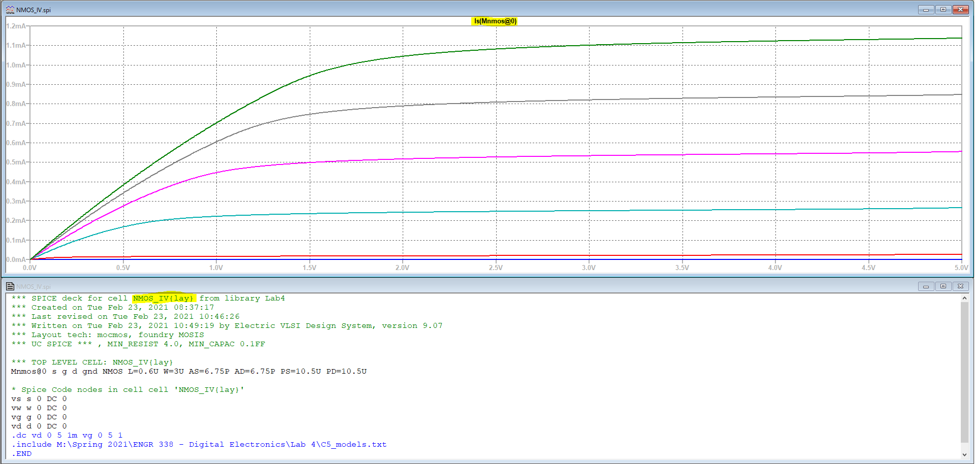
Figure 4. NMOS_IV{lay} LTSpice waveform results from "Is" probed
The same process was done for the PMOS with the development of the schematic and layout which can be seen in Figures 5 and 6.
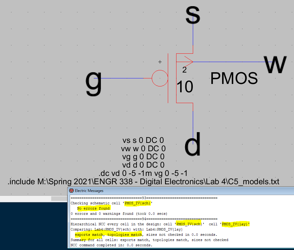
Figure 5. PMOS_IV{sch} final design with LTSpice code and DRC/NRC scans passed
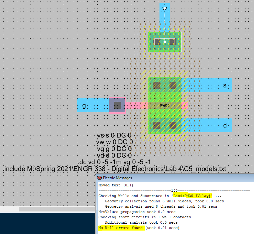
Figure 6. PMOS_IV{lay} final design with LTSpice code and ERC scan passed
Next were the LTSpice waveforms
generated by both of these designs. These two waveforms can be seen in
Figures 7 and 8. It can be noted that both of these are smaller than
the NMOS waveforms; the scale of the NMOS waveforms are 0A - 1.2mA while PMOS waveforms are defaulted to 0A - 700uA.
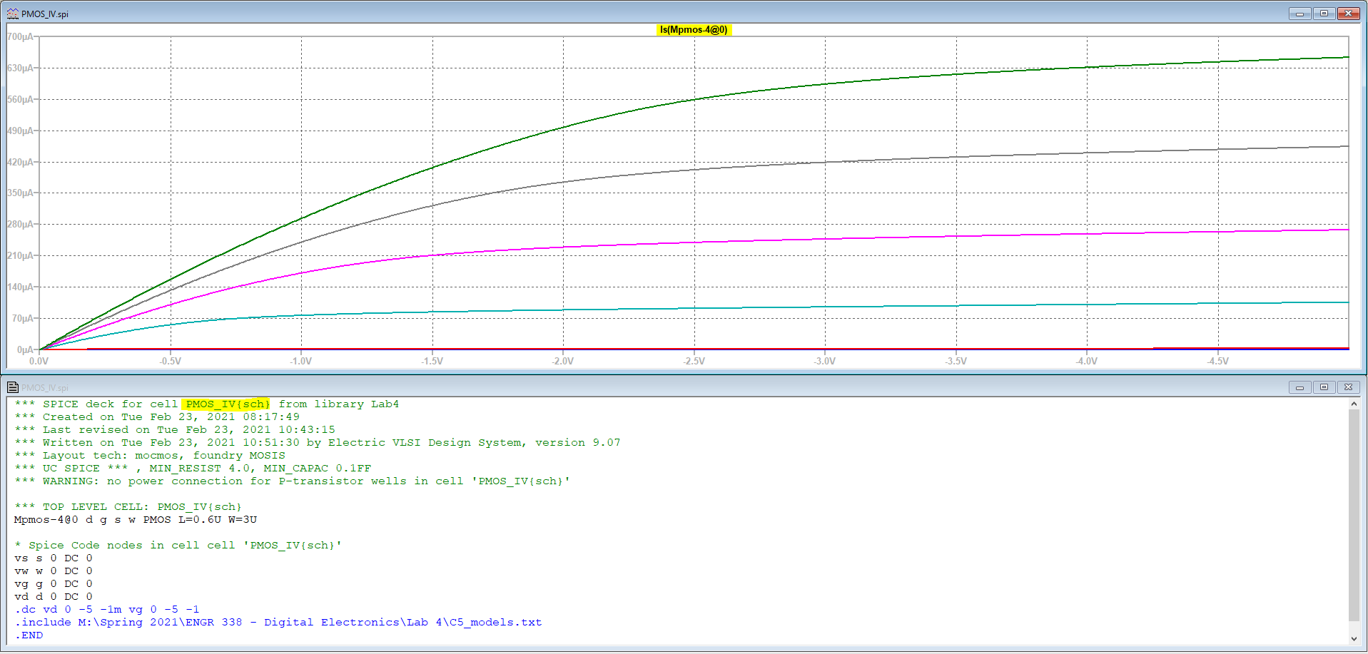
Figure 7. PMOS_IV{sch} LTSpice waveform results from "Is" probed
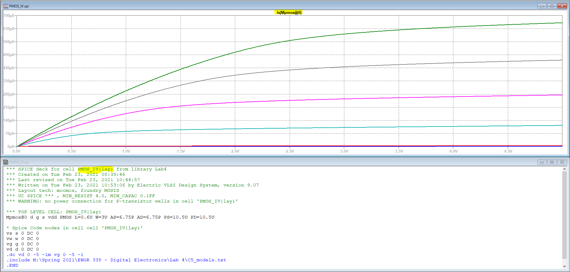
Figure 8. PMOS_IV{lay} LTSpice waveform results from "Is" probed
Discussion
This was a simple lab to execute but harder to understand;
I've rewatched the lectures and videos online to try and help me
understand the waveforms, NMOS, PMOS, and BJTs. For what ever reason,
it just isn't clicking for me, even with all the drawn out diagrams
(I'm a visual learner too). I think the next thing that would help me
understand it better would be to execute this lab in some sort of
physical setting. Regardless, it's obvious that the intended outcome
was acheived via the waveforms because I at least recognize those from
our class and the various regions from them like the cut-off,
saturation, and linear region(s).