ENGR338 Lab 2021 Spring
Lab 3 Layout the R-2R DAC
Tyrone Bracker
tabrackeryazzie@fortlewis.edu
Lab 3 Report: Developing Layouts in EletricVLSI
Introduction
As the third lab in the series, this one once again
introduced new methods and expanded the functionality of ElectricVLSI
for me. Developing and implementing different layouts as well as a subcell in Electric were the two newer features emphasized in this lab. The R_2R_Ladder
design from previous labs was also used to create a the new subcell
which would later go into creating larger designs. Various design
choices like the width and length of n-well resistors was also
explained and solved using simple math. Other than the three things
mentioned, lab 3 was relatively easy to follow along with.
Materials and Methods
Task 1 had me taking the top of the R_2R_Ladder schematic as the base
of my new subcell design. From here all I had to do was create a new
schematic and add another 'Off-Page' port; in total, I had three 10k
n-well resistors and three off-page ports labeled: "Left", "Right", and
"Down", in there respective locations. After the schematic was done, an
icon was alos created. The final step was to create a larger schematic
and icon called "R_2R_Ladder_V2" built from the smaller parts of
the "R_2R_Subcell" schematic and icon. This was acheived by copy and
pasting the parts then connecting them together to once again, form a
ladder.
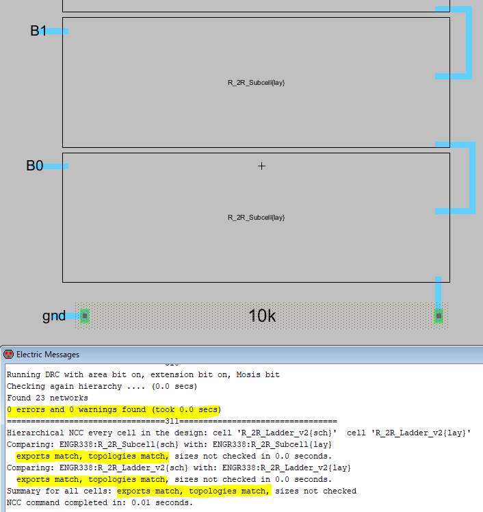
Both groups R_2R_Ladder_V2 and R_2R_Subcell
had schematics and icons, but not layouts. Task 2 was all about
developing layouts for both of these. The subcell group recieved the
first layout development with specific spacing, length, and width,
constraints. This design, which can be seen in Figure 1, was once again
used to build a larger layout design for R_2R_Ladder_V2.
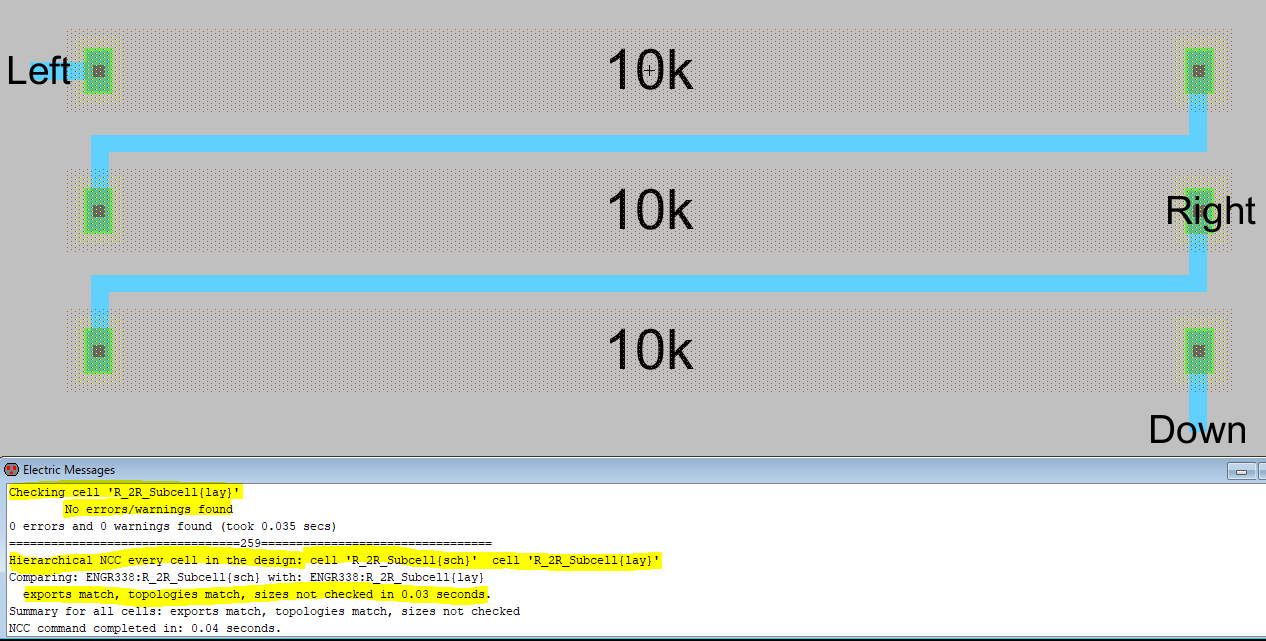
Figure 1. R_2R_Subcell{lay} design used to build 2_R2_Ladder_V2{lay}
Results
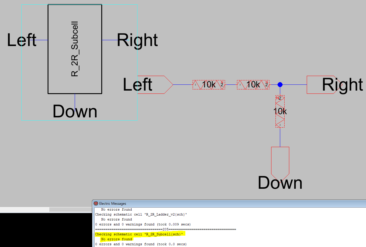
First came the schematic and icon for R_2R_Subcell using the top
of the previous ladder. The final designs of these can be seen in Figure 2.
Figure 2. R_2R_Subcell{sch} and {ic} with a clean DRC scan
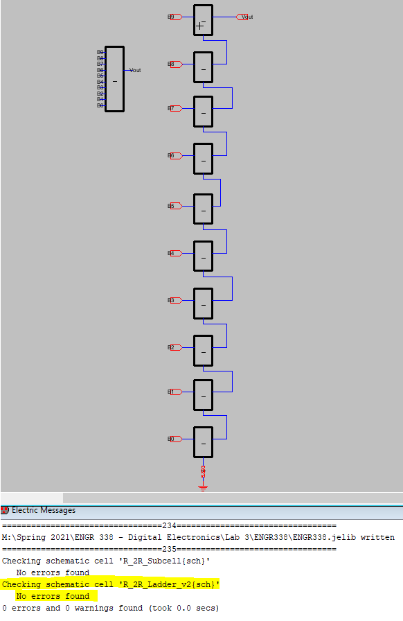
Once the components from the Subcell group was done, R_2R_Ladder_V2 was created from those components. Both schematic and icon for the new ladder can be seen in the following figure. This is also where Task 1 ended.
Figure 3. R_2R_Ladder_V2{sch} and {ic} with a clean DRC scan
Task 2 followed the same
formula of creating a small layout in the subcell and building a larger
layout for the ladder. The end of the layout for R_2R_Ladder_v2 can be
seen in Figure 4; this figure also shows the layout part created in
R_2R_Subcell.
Figure 4. The bottom of R_2R_Ladder_V2{lay} with clean DRC and NCC scans
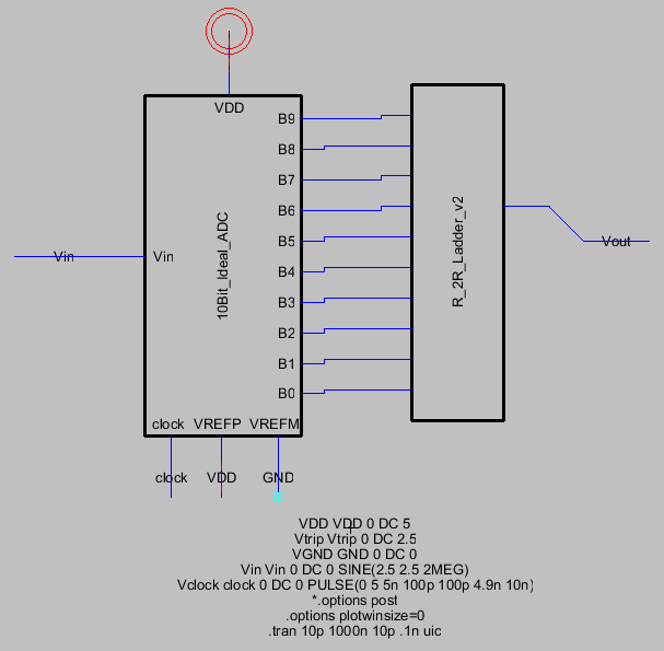
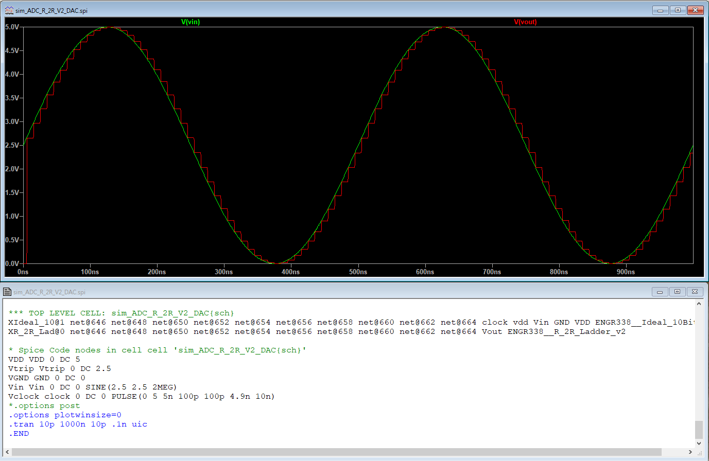
To make sure the designs worked properly, I connected the newer version
of the ladder to the ideal ADC design and ran it through LTSpice. The
new schematic and LTSpice wavefrom can be seen in Figures 5 and 6.
Figure 4. New schematic called "sim_ADC_R_2R_V2_DAC{sch}"
Figure 6. LTSpice Waveform results from sim_ADC_R_2R_V2_DAC{sch}
Discussion
This lab was a good way of introducing a new way of building larger
schematics, icons, and layouts. It's a safer than building everything
all at once and having to rely on one whole design. It's also a good
practice to have building-blocks to have at your disposal for future
projects or just individal inspection. Overall I think this was a great
way to showcase that idea/concept in Electric.